A high-bandwidth cmos APD optoelectronic device operating in the visible light band

A photoelectric device and visible light technology, applied in the field of visible light detection, can solve problems such as high bandwidth and low dark current, and achieve the effect of reducing dark current and improving bandwidth

Active Publication Date: 2020-12-01
CHONGQING UNIV OF POSTS & TELECOMM
View PDF9 Cites 0 Cited by
  • Summary
  • Abstract
  • Description
  • Claims
  • Application Information

AI Technical Summary

Problems solved by technology

The traditional APD device design technology is only optimized on the P+ / N well, ignoring the drift velocity of the photogenerated electron carriers and the reasonable use of the STI guard ring, so it cannot achieve high bandwidth while maintaining low dark current

Method used


Image

  • A high-bandwidth cmos APD optoelectronic device operating in the visible light band
  • A high-bandwidth cmos APD optoelectronic device operating in the visible light band
  • A high-bandwidth cmos APD optoelectronic device operating in the visible light band

Examples


Embodiment Construction

[0025] The technical solutions in the embodiments of the present invention will be described in detail below with reference to the drawings in the embodiments of the present invention. The described embodiments are merely a part of the embodiments of the invention.

[0026] The technical solution to solve the above technical problem is:

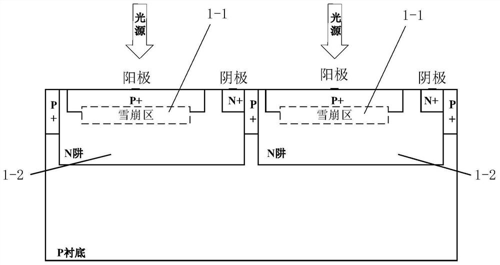
[0027] like figure 1 The design technology diagram showing the conventional CMOS APD photoelectric device. As can be seen from the figure, in the design technique, the PN doping is composed of a heavy doped p + layer and a lightly doped N-well, and the avalanche region (corresponding to the 1-1 region in the figure) is located at the PN junction, the P-well below the avalanche area. It is the main light absorbing area (1-2 region in the figure). The P + on both sides of the PN junction is used as a protective ring, avoiding the premature edge breakdown of the device. The working principle of the APD photoelectric device is an incident light injec...


PUM


Abstract

The invention relates to a high-bandwidth CMOS APD photoelectric device working in a visible light waveband. The high-bandwidth CMOS APD photoelectric device comprises a P substrate, and two deep N wells stacked on the P substrate, two P well layers are stacked on the deep N wells, one N+ layer and one P+ layer are stacked on each P well layer, a PN junction is formed by the heavily doped N+ layers and the lightly doped P well layers, namely an avalanche region is formed, the avalanche region comprises a first avalanche region and a second avalanche region, and is provided with two illumination windows, when a light source is emitted into the device and is absorbed by a light absorption region, a photon-generated carrier is generated, and the photon-generated carrier moves to the first avalanche region and the second avalanche region under the action of an electric field to participate in multiplication; and STI guard rings are added at two ends of the gap of the P well layers. The design technology is designed from two aspects of the PN junction and the size of the depletion region, the dark current of the device is reduced, and the bandwidth of the device is improved.

Description

Technical field [0001] The present invention belongs to the field of visible light detection, and the design technology design of APD optoelectronic devices involves a new design technology with high bandwidth CMOS APD photoelectric device. Background technique [0002] Avalanche photodio is a photodetector that enables high sensitivity and high bandwidth. It has a multiplication electron, hole. The basic design technology of CMOS APD is similar to the basic design technology of ordinary PN junctions, but new design techniques can be effectively improved during design, but can effectively improve the work bandwidth of the device. The CMOS APD working in the linear zone is widely used in its low voltage and low cost features, which are widely used in the Internet of Things, CD (CD-ROM), digital multi-function optical disc (DVD), and Blu-ray disc. [0003] The device design technology of the CMOS APD can be divided into two categories according to the type of PN. One is an electron...

Claims


Application Information

Patent Timeline
Patent Type & Authority Patents(China)
IPC IPC(8): H01L31/107H01L31/0352
CPCH01L31/035272H01L31/107
Inventor 王巍曾虹谙赵元遥毛鼎昌王冠宇
Owner CHONGQING UNIV OF POSTS & TELECOMM
Why Eureka
Try Eureka