High-bandwidth CMOS APD device

A high-bandwidth and device technology, applied in the field of visible light detection, can solve the problems of inability to achieve high-bandwidth, small size, ignoring the rational use of photogenerated electron carriers, etc., and achieve the effect of small size, reduced electrode distance, and improved bandwidth.

Pending Publication Date: 2020-05-08
CHONGQING UNIV OF POSTS & TELECOMM
View PDF6 Cites 0 Cited by
  • Summary
  • Abstract
  • Description
  • Claims
  • Application Information

AI Technical Summary

Problems solved by technology

The traditional APD device design technology is only optimized on the P+ / N well, ignoring the reasonable use of the horizontal and vertical crossing distance of photogenerated electron carriers, so it cannot achieve high bandwidth while maintaining a small size

Method used


Image

  • High-bandwidth CMOS APD device
  • High-bandwidth CMOS APD device
  • High-bandwidth CMOS APD device

Examples


Embodiment Construction

[0032] The technical solutions in the embodiments of the present invention will be described clearly and in detail below with reference to the drawings in the embodiments of the present invention. The described embodiments are only some of the embodiments of the invention.

[0033] The technical scheme that the present invention solves the problems of the technologies described above is:

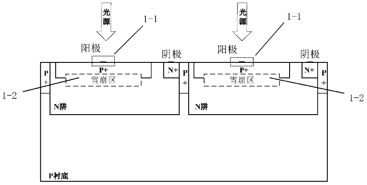
[0034] Such as figure 1Shown is a design technical diagram of a conventional CMOS APD optoelectronic device. It can be seen from the figure that in this design technology, the PN junction is composed of a heavily doped P+ layer and a lightly doped N well. The avalanche region (corresponding to the 1-2 region in the figure) is located at the PN junction, and the P layer is above the avalanche region. at the electrode (corresponding to the 1-1 area in the figure). The working principle of the APD photoelectric device is that when the incident light enters the device and is absorbed by the l...


PUM


Abstract

The invention requests to protect a high-bandwidth CMOS APD device, a conventional CMOS APD structure does not consider a bandwidth improvement method except a depletion layer, and only considers reduction of transverse and longitudinal widths of the depletion layer to reduce minority carrier transit time. In order to further improve the bandwidth of the CMOS APD, therefore, the length L from theelectrode to the boundary of the N+ layer of the illumination region and the electrode area are adjusted to increase. Under the condition of avalanche multiplication, for a P+/N well type CMOS APD, the hole lateral carrier transit distance is reduced by adjusting the distance L between a cathode electrode on N+ and the boundary and the size of the electrode, and then the carrier transit time is prolonged; and, for the P+/N well type CMOS APD, the hole lateral electron carrier transit distance is reduced by adjusting the distance L between the anode electrode on the P+ and the boundary and theelectrode size, so that the carrier transit time is prolonged, and the bandwidth is increased. According to the improved technology, the electrode distance and the electrode area size are improved, carriers are reduced, and the bandwidth is increased.

Description

technical field [0001] The invention belongs to the technical field of visible light detection, and in particular relates to a high-bandwidth CMOS APD device. Background technique [0002] Avalanche Photodiode (Avalanche Photodiode) is a photodetector capable of high sensitivity and high bandwidth. It has electrons, holes that are multiplied by absorbing the optical signal in the depletion layer by utilizing avalanche breakdown. The basic design technology of CMOS APD is similar to the basic design technology of ordinary PN junction, but the new design technology is adopted in the design process, which can effectively improve the working bandwidth of the device. CMOS APDs operating in the linear region are widely used in the Internet of Things, compact disc read-only memory (CD-ROM), digital versatile disc (DVD) and Blu-ray disc due to its low voltage and low cost. [0003] The device design technology of CMOS APD can be divided into two categories according to the type of...

Claims


Application Information

Patent Timeline
Patent Type & Authority Applications(China)
IPC IPC(8): H01L31/112H01L31/113H01L27/02H01L29/06
CPCH01L31/112H01L31/1136H01L27/0203H01L29/0603
Inventor 王巍曾虹谙毛鼎昌周怡王方王冠宇冯世娟
Owner CHONGQING UNIV OF POSTS & TELECOMM
Why Eureka
Try Eureka