CMOS APD photoelectric device with low dark current

A photoelectric device and dark current technology, applied in the direction of electrical components, semiconductor devices, circuits, etc., can solve the problems of low dark current, failure to achieve guarantee, ignoring the reasonable use of photo-generated electron carrier drift distance, etc., to reduce the vertical width, Effect of reducing dark current, reducing number and range

Active Publication Date: 2021-04-09
重庆中易智芯科技有限责任公司
View PDF9 Cites 1 Cited by
  • Summary
  • Abstract
  • Description
  • Claims
  • Application Information

AI Technical Summary

Problems solved by technology

The traditional APD device design technology will add STI protection ring optimization on both sides of the cathode and anode, ignoring the drift distance of photogenerated el

Method used


Image

  • CMOS APD photoelectric device with low dark current
  • CMOS APD photoelectric device with low dark current
  • CMOS APD photoelectric device with low dark current

Examples


Embodiment Construction

[0025] The technical solutions in the embodiments of the present invention will be described clearly and in detail below with reference to the drawings in the embodiments of the present invention. The described embodiments are only some of the embodiments of the invention.

[0026] The technical scheme that the present invention solves the problems of the technologies described above is:

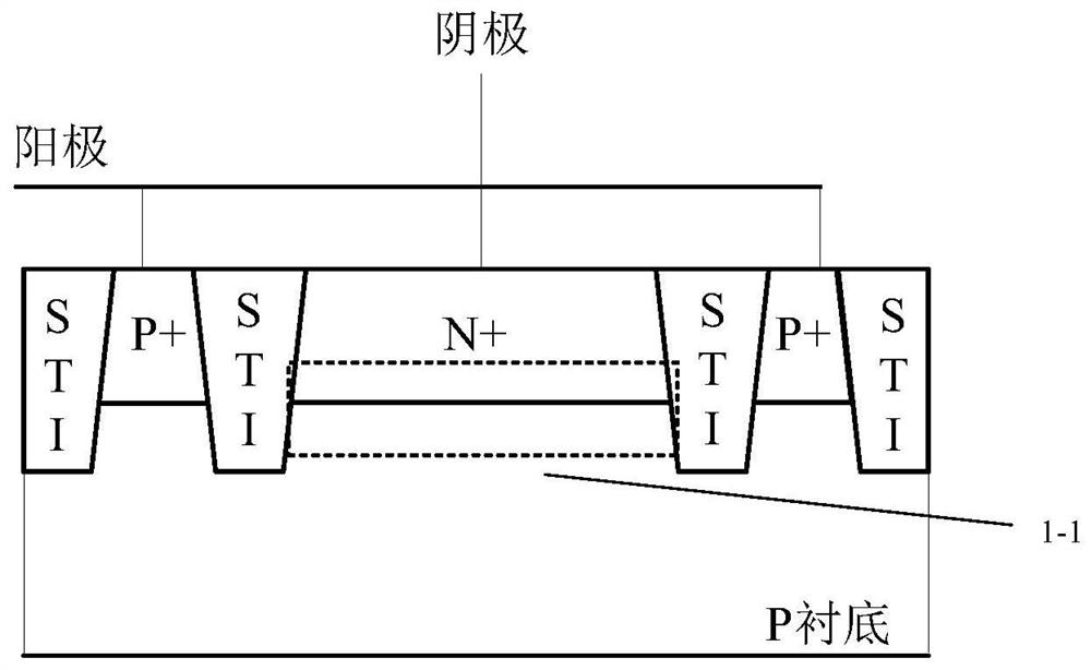
[0027] Such as figure 1 Shown is a design technical diagram of a conventional CMOS APD optoelectronic device. It can be seen from the figure that in this design technology, the PN junction is composed of a heavily doped P+ layer and a lightly doped N well, the avalanche region (corresponding to the 1-1 region in the figure) is located at the PN junction, and the P lining The bottom is the main light-absorbing region. The P+ on both sides of the PN junction acts as a protection ring to prevent premature edge breakdown of the device and the entry of diffuse carriers on both sides. The work...


PUM


Abstract

The invention discloses a CMOS APD photoelectric device with low dark current, and belongs to the field of semiconductor photoelectric devices. The device structure comprises a P substrate and further comprises a P trap which is subjected to ion implantation on the P substrate, an N+ layer and two P+ layers are subjected to ion implantation on the P trap, the N+ layer is a cathode, and the P+ layers are anodes. The heavily doped N+ layer and the lightly doped P well layer form a PN junction, namely an avalanche region is formed, an illumination window is arranged, when a light source is emitted into the device and absorbed by the light absorption region, photon-generated carriers are generated, and the photon-generated carriers move to the avalanche region under the action of an electric field to participate in multiplication; STI protection rings are doped at the two ends of the gap of the P well layer, small-size STI protection rings are doped at the two sides of the N + layer, and due to reasonable arrangement of STI, reduction of dark current can be guaranteed, and photocurrent can be effectively detected; and the photoelectric effect and the capacitance are optimized on the design of the device electrode. The design technology is designed from three aspects of PN junction, STI protection ring and electrode arrangement, so the dark current of the device is reduced, it is ensured that the photocurrent can be detected, and the capacitance is reduced.

Description

technical field [0001] The invention belongs to the field of semiconductor devices, relates to the design technology design of an APD optoelectronic device, in particular to the design of a low dark current CMOS APD optoelectronic device. Background technique [0002] Avalanche Photodiode (Avalanche Photodiode) is a photodetector capable of high sensitivity and high bandwidth. It has the function of absorbing the optical signal in the depletion layer by using the avalanche breakdown effect to generate multiplied carrier electrons and holes. The basic design technology of CMOS APD is similar to the basic design technology of ordinary PN junction, but adopting new design technology in device structure design can effectively improve the working bandwidth of the device and reduce the dark current of the device. CMOSAPD operating in the linear region is widely used in the Internet of Things, CD-ROM, DVD and Blu-ray due to its low voltage and low cost. [0003] Semiconductor dev...

Claims


Application Information

Patent Timeline
IPC IPC(8): H01L31/107H01L31/0224H01L31/02
CPCH01L31/107H01L31/022408H01L31/02027
Inventor 霍军王巍黎淼丁立樊琦赵汝法袁军
Owner 重庆中易智芯科技有限责任公司
Why Eureka
Try Eureka