A method for detecting wafer ups and downs and a grinding device

A detection method, wafer technology, applied in the direction of measuring device, optical device, grinding feed movement, etc., to achieve the effect of preventing the number of processes from increasing

Pending Publication Date: 2018-09-25
DISCO CORP
View PDF4 Cites 0 Cited by
  • Summary
  • Abstract
  • Description
  • Claims
  • Application Information

AI Technical Summary

Problems solved by technology

[0005] Therefore, in the case of grinding a wafer using a grinding device, there is a problem in that the number of steps for processing can be prevented from increasing without taking out the wafer from the grinding device and measuring the waviness with another measuring device.

Method used


Image

  • A method for detecting wafer ups and downs and a grinding device
  • A method for detecting wafer ups and downs and a grinding device
  • A method for detecting wafer ups and downs and a grinding device

Examples


Embodiment Construction

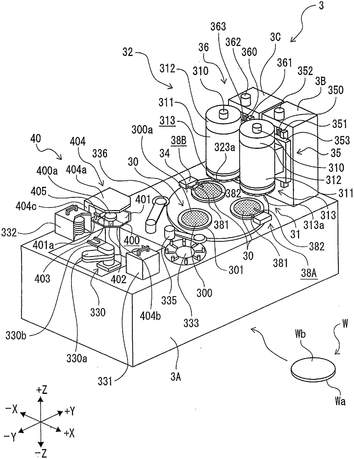
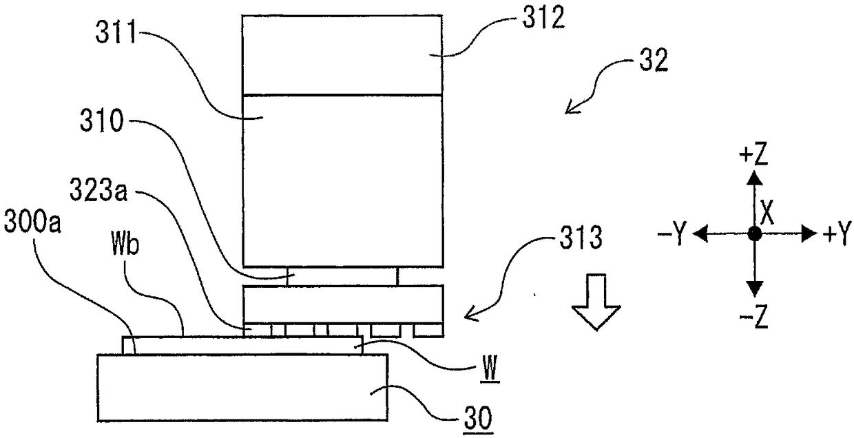
[0019] figure 1 The shown grinding device 3 is a device that performs grinding processing on the wafer W sucked and held by the chuck table 30 . Thinned by grinding figure 1 The illustrated wafer W is, for example, a circular semiconductor wafer made of silicon, and on the front surface Wa of the wafer W, a plurality of devices are formed in grid-like regions partitioned by dividing lines. The front Wa is protected by, for example, a not-shown protective tape. The back surface Wb of the wafer W is a ground surface to be ground.

[0020] The front side (the −Y direction side) on the base 3A of the grinding apparatus 3 is an area where the wafer W is attached to and detached from the chuck table 30 by the robot 330 capable of transferring the wafer W. The rear side (+Y direction side) on the susceptor 3A is held on the chuck table 30 by a rough grinding unit 31 for rough grinding the wafer W or a finish grinding unit 32 for finishing the wafer W. Grinding area on wafer W.

...


PUM


Abstract

A method for detecting wafer ups and downs and a grinding device are provided. When a wafer is ground using the grinding device, it is not necessary to take the wafer out of the grinding device and measure ups and downs by another measuring device, thereby preventing an increase in the number of processing steps. The method for detecting wafer ups and downs is provided and includes a holding stepin which a wafer (W) is held on a holding workbench (400); a contact step in which a flat transparent plate (50) is brought into contact with the wafer (W) held on the holding workbench (400); and anirradiating step in which light is irradiated from the transparent plate (50) side, and ups and downs of the wafer (W) are detected through interference fringes (R) generated in the irradiating step.

Description

technical field [0001] The present invention relates to a method and a grinding device for detecting wafer fluctuations. The detection method detects the fluctuations of the ground surface of the wafer before grinding or the fluctuation of the ground surface of the wafer after grinding. The grinding device can The wafer is ground and this undulation can be detected. Background technique [0002] A plate-like workpiece such as a silicon wafer is ground and thinned to a predetermined thickness by a grinding device (for example, refer to Patent Document 1), and then divided into individual device chips by a cutting device or the like, and is used in various electronic equipment, etc. [0003] Patent Document 1: Japanese Patent Laid-Open No. 2009-094247 [0004] When the processing conditions during grinding are not suitable or when there is any abnormality in the various components of the grinding device or the grinding tool, there may be a cause of failure on the ground surf...

Claims


Application Information

Patent Timeline
Patent Type & Authority Applications(China)
IPC IPC(8): H01L21/66B24B7/22B24B27/00B24B41/00B24B41/06B24B49/12G01B11/30
CPCH01L22/12G01B11/303B24B7/228B24B27/0023B24B27/0076B24B41/005B24B41/06B24B49/12
Inventor 清野敦志
Owner DISCO CORP
Why Eureka
Try Eureka