Vertical super-junction double diffused metal oxide semiconductor device and manufacturing method thereof

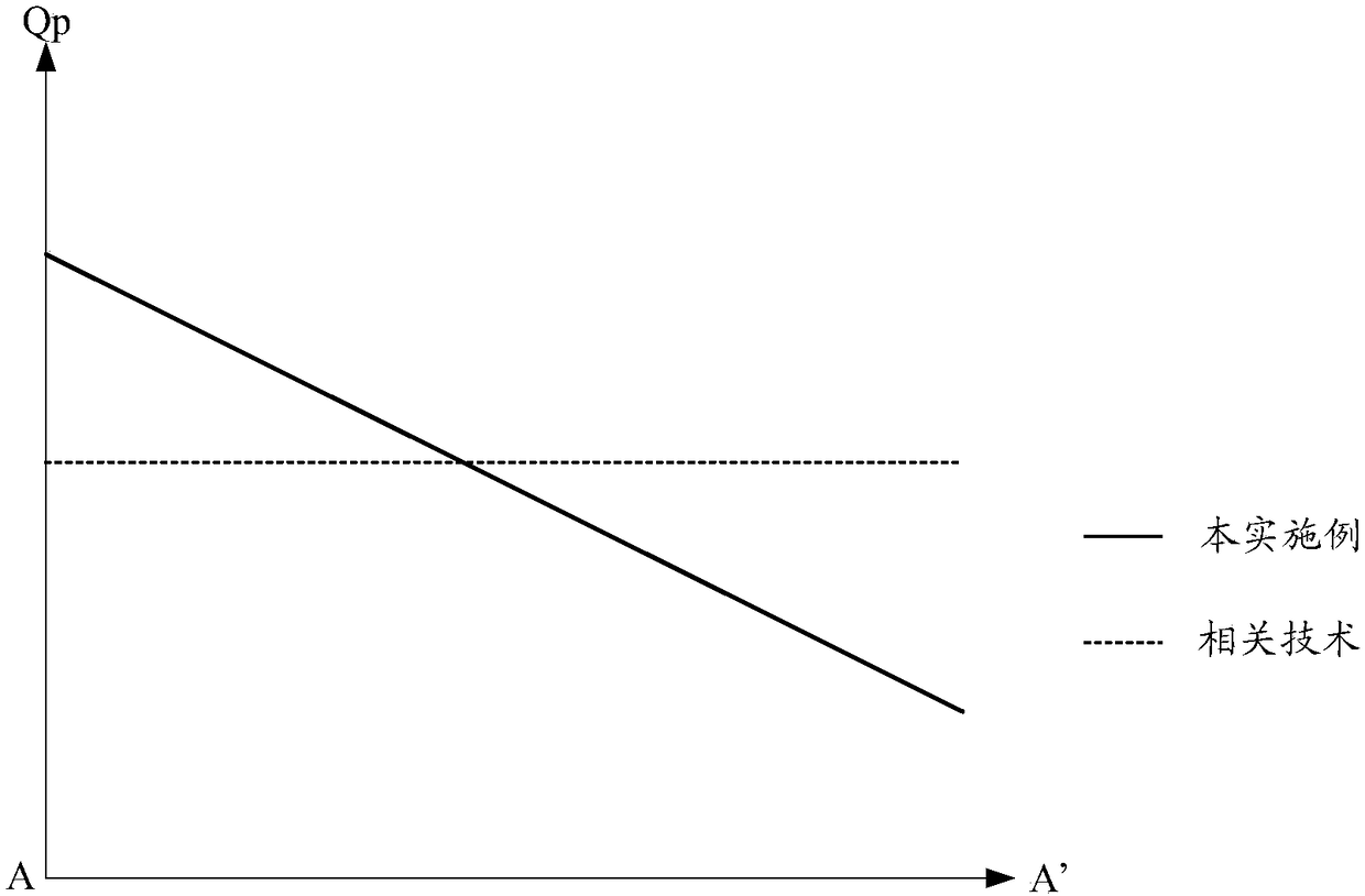
A technology of oxide semiconductor and manufacturing method, which is applied in semiconductor/solid-state device manufacturing, semiconductor devices, electrical components, etc., can solve the problems of high cost, reduce the degree of Qp/Qn variation, disadvantageous device thinning, etc., so as to reduce the manufacturing cost. , Improve the electrical performance, the requirements of the production process are simple

Inactive Publication Date: 2018-09-25
WUXI CHINA RESOURCES HUAJING MICROELECTRONICS
View PDF3 Cites 0 Cited by
  • Summary
  • Abstract
  • Description
  • Claims
  • Application Information

AI Technical Summary

Problems solved by technology

And the BV with a large fluctuation range has a great adverse effect on the super junction semiconductor device.
[0003] In order to reduce the fluctuation of BV caused by the change of Qp / Qn, one way in related technologies is to precisely control the ratio of Qp to Qn by improving the manufacturing precision in the process, but this requires high-precision manufacturing and testing equipment, and the cost Too high; another way is to reduce the total amount of Qp and Qn, thereby reducing the degree of variation of Qp / Qn, but in order to obtain sufficient internal resistance of the component, it is necessary to increase the area or volume of the device, which is not conducive to the thinning of the device

Method used


Image

  • Vertical super-junction double diffused metal oxide semiconductor device and manufacturing method thereof
  • Vertical super-junction double diffused metal oxide semiconductor device and manufacturing method thereof
  • Vertical super-junction double diffused metal oxide semiconductor device and manufacturing method thereof

Examples


Embodiment Construction

[0039] Reference will now be made in detail to the exemplary embodiments, examples of which are illustrated in the accompanying drawings. When the following description refers to the accompanying drawings, the same numerals in different drawings refer to the same or similar elements unless otherwise indicated. The implementations described in the following exemplary examples do not represent all implementations consistent with the present invention. Rather, they are merely examples of apparatuses and methods consistent with aspects of the invention as recited in the appended claims.

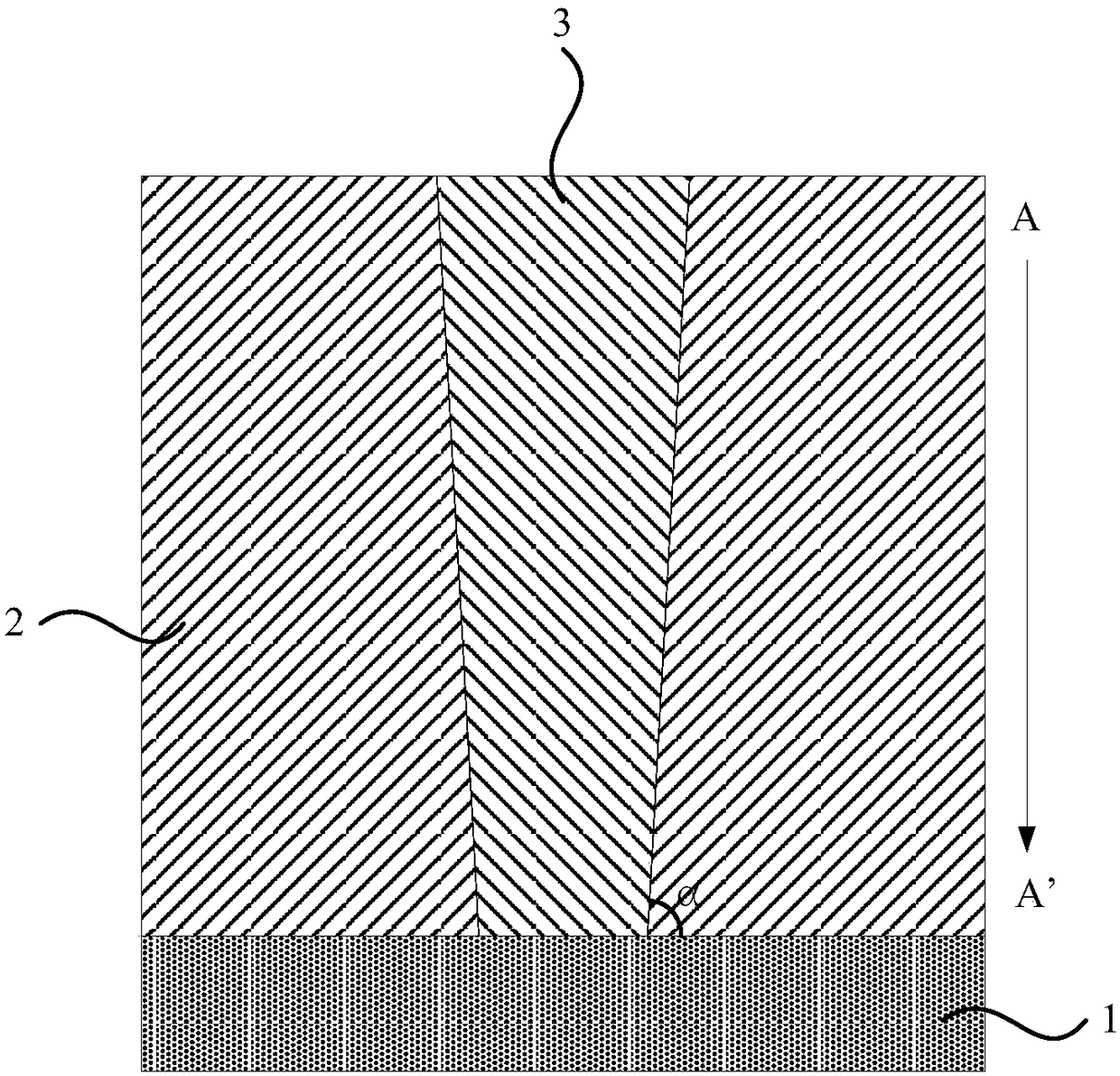
[0040] figure 1 It is a schematic structural diagram of a vertical superjunction double diffused metal oxide semiconductor device according to an embodiment of the present invention, and the semiconductor device may include a plurality of vertical superjunction double diffused metal oxide semiconductor units, such as figure 1 As shown, the vertical superjunction double diffused metal oxide semi...


PUM


Abstract

The invention relates to a vertical super-junction double diffused metal oxide semiconductor device, which comprises a plurality of vertical super-junction double diffused metal oxide semiconductor units. Each vertical super-junction double diffused metal oxide semiconductor unit comprises a substrate, a first-type epitaxial layer and a second-type epitaxial layer, wherein the first-type epitaxiallayer is formed at one side of the substrate; and the second-type epitaxial layer is formed in the first-type epitaxial layer, and the width of the second-type epitaxial layer increases gradually ina direction away from the substrate. According to the technical scheme of the invention, the width of the P-type epitaxial layer is set to increase gradually towards the direction away from the substrate, so that influences imposed on the breakdown voltage by the change of Qp/Qn can be reduced, and the electrical performance of the semiconductor device is improved. In addition, the Qp/Qn can be changed within a larger range under the same breakdown voltage, so that requirements for the manufacturing process are relatively simple, and the manufacturing cost is easy to be reduced.

Description

technical field [0001] The invention relates to the field of semiconductor technology, in particular to a vertical superjunction double-diffused metal oxide semiconductor device and a manufacturing method of the vertical superjunction double-diffused metal oxide semiconductor device. Background technique [0002] In the current super junction semiconductor device, the breakdown voltage BV will fluctuate violently with the change of Qp / Qn, where Qp is the charge amount of the P epitaxial layer, and Qn is the charge amount of the N epitaxial layer. The BV with large fluctuations has a large adverse effect on the super junction semiconductor device. [0003] In order to reduce the fluctuation of BV caused by the change of Qp / Qn, one way in related technologies is to precisely control the ratio of Qp to Qn by improving the manufacturing precision in the process, but this requires high-precision manufacturing and testing equipment, and the cost Too high; another way is to reduce...

Claims


Application Information

Patent Timeline
Patent Type & Authority Applications(China)
IPC IPC(8): H01L29/78H01L29/06H01L21/336
CPCH01L29/0611H01L29/0684H01L29/66666H01L29/7827H01L29/0634H01L29/7802
Inventor 钟圣荣郑芳
Owner WUXI CHINA RESOURCES HUAJING MICROELECTRONICS
Why Eureka
Try Eureka