
Embedded chip packaging method adopting glue spraying at groove bottoms

A chip packaging and glue spraying technology, used in semiconductor/solid-state device parts, electrical components, electric solid-state devices, etc., can solve the problem that the chip that cannot be DAF film is removed from the cutting film, the cost of DAF film material is high, and it cannot be embedded. Chip and other problems, to achieve the effect of low cost, fast operation efficiency, and reduced chip spacing

Inactive Publication Date: 2018-09-28
HUATIAN TECH KUNSHAN ELECTRONICS
View PDF5 Cites 7 Cited by
  • Summary
  • Abstract
  • Description
  • Claims
  • Application Information

AI Technical Summary

Problems solved by technology

[0004] One of the key processes of silicon-based fan-out technology is chip placement. This packaging process uses a chip mounter to paste the cut chip with DAF film into the groove of the substrate, but the existing chip mounter uses a gas sensor to sense For chips, the range that can hold chips with DAF film is above 0.5mm×0.5mm. For smaller size chips, a smaller suction nozzle is required, and the chip with DAF film cannot be removed from the cutting film. Therefore, it is impossible to embed the chip
In addition, this packaging process uses DAF film to embed the chip in the groove of the substrate. Since the DAF film is a solid film structure, it is easy to generate bubbles when heated after pasting, and there are phenomena such as voids and glue overflow, and the material cost of the DAF film is relatively high. , work efficiency is slow
In addition, in this packaging process, grooves are made on the substrate. In order to make the surface of the wafer more uniform and prevent chips from protruding, the bottom of the groove is required to have a higher level. However, due to the uniformity of the substrate, the etched surface The depth of the ring is deeper than the depth of the etched inner ring, and the thickness of the DAF film is consistent, which brings a huge challenge to the etching accuracy

Method used


Image

  • Embedded chip packaging method adopting glue spraying at groove bottoms
  • Embedded chip packaging method adopting glue spraying at groove bottoms
  • Embedded chip packaging method adopting glue spraying at groove bottoms

Examples


Embodiment Construction

[0027] In order to understand the technical content of the present invention more clearly, the following examples are given in detail, the purpose of which is only to better understand the content of the present invention but not to limit the protection scope of the present invention. The components in the structures in the drawings of the embodiments are not scaled according to the normal scale, so they do not represent the actual relative sizes of the structures in the embodiments.

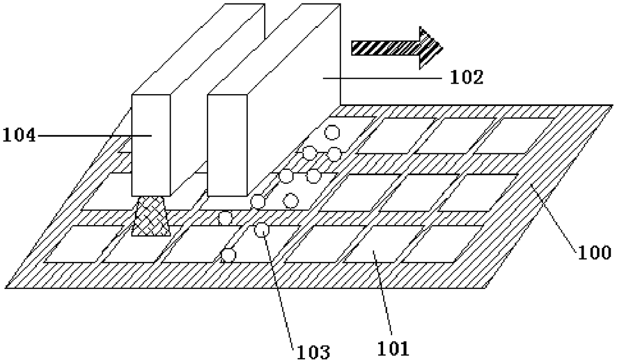
[0028] Such as figure 1 As shown, an embedded chip packaging method of spraying glue at the bottom of the groove is implemented according to the following steps:

[0029] A. Etch a groove 101 on the substrate 100 by an etching method;

[0030] B. Use glue spraying equipment to spray UV glue in the groove, and control the glue spraying head 102 of the glue spraying equipment to spray UV glue to the bottom of the groove in the form of glue droplets 103 for attaching chips , and control the thick...


PUM


Abstract

The invention discloses an embedded chip packaging method adopting glue spraying at groove bottoms. The method comprises the following steps: spraying UV glue on an area, where a chip is to be mounted, at the bottom of each groove in the form of glue droplets through special glue spraying equipment; controlling the fixed-point glue spraying thickness of a glue spraying nozzle in the areas; and during the UV glue spraying, using a UV light source to illuminate the sprayed UV glue for UV curing, so that shape solidification is achieved. The method provided by the invention has the advantages that the applicability for chips with smaller dimensions is achieved, so that the problem that a chip with a DAF, of which the dimensions are 0.5mm x 0.5mm or below, cannot be held by the conventional packaging equipment is solved, high etching uniformity of the grooves on a substrate is achieved, and holes, excessive glue and other problems on the DAF that easily occur during chip mounting are avoided; and moreover, compared with the method adopting the DAF, the method provided by the invention achieves lower cost, a simpler process, and higher operation efficiency (the UPH can reach 70 pcs / h).

Description

technical field [0001] The invention relates to the technical field of semiconductor packaging, in particular to an embedded chip packaging method by spraying glue at the bottom of a groove. Background technique [0002] Wafer-level fan-out packaging technology is an important integration technology that continues and surpasses Moore's Law, and is the focus of technology competition in the international packaging and testing field. Chip embedded substrate technology is one of the important technologies applied in wafer-level fan-out packaging technology . Wafer-level fan-out technology was invented by Infineon. The main technical feature is to borrow the area of ​​the molding compound to make the surface of the chip have enough space for wiring and ball planting, so that the pitch of the solder balls meets the requirements of PCB interconnection. The specific method includes transferring the chip to the substrate, embedding the chip into the molding compound through plastic...

Claims


Application Information

Patent Timeline
Patent Type & Authority Applications(China)
IPC IPC(8): H01L23/488H01L21/48
CPCH01L24/83H01L21/4803H01L2224/8322H01L2224/83024H01L2224/18H01L2924/15153H01L2224/12105H01L2224/73267
Inventor 马书英
Owner HUATIAN TECH KUNSHAN ELECTRONICS
Learn More