Gallium nitride light emitting diode and preparation method thereof

A technology of light-emitting diodes and gallium nitride, which is applied in the direction of electrical components, circuits, semiconductor devices, etc., can solve problems such as poor structural stability, low luminous brightness, and poor shock resistance, and achieve improved fastness, improved luminous efficiency, and reduced The effect of defect density

Active Publication Date: 2018-09-28
RUGAO DACHANG ELECTRONICS
View PDF5 Cites 2 Cited by
  • Summary
  • Abstract
  • Description
  • Claims
  • Application Information

AI Technical Summary

Problems solved by technology

[0002] Light emitting diode (light emitting diode) abbreviation and commonly known as LED is a semiconductor solid light emitting device; it uses a solid chip as a light emitting material, recombines through carriers in the semiconductor, and releases excess energy to cause photon emission, emitting red and yellow light. , blue, green, blue, orange, purple, white visible light or invisible light; the light-emitting diodes in the prior art have a complicated structure, complicated installation, and poor structural stability. When in use, the shock resistance is poor. At the same time, the prior art The light-emitting diode in the present invention has high power consumption and low luminous brightness, which is far from meeting people's needs. Therefore, it is necessary to design a gallium nitride light-emitting diode and its preparation method

Method used


Image

  • Gallium nitride light emitting diode and preparation method thereof
  • Gallium nitride light emitting diode and preparation method thereof
  • Gallium nitride light emitting diode and preparation method thereof

Examples


Embodiment Construction

[0023] The following will clearly and completely describe the technical solutions in the embodiments of the present invention with reference to the accompanying drawings in the embodiments of the present invention. Obviously, the described embodiments are only some, not all, embodiments of the present invention. Based on the embodiments of the present invention, all other embodiments obtained by persons of ordinary skill in the art without making creative efforts belong to the protection scope of the present invention.

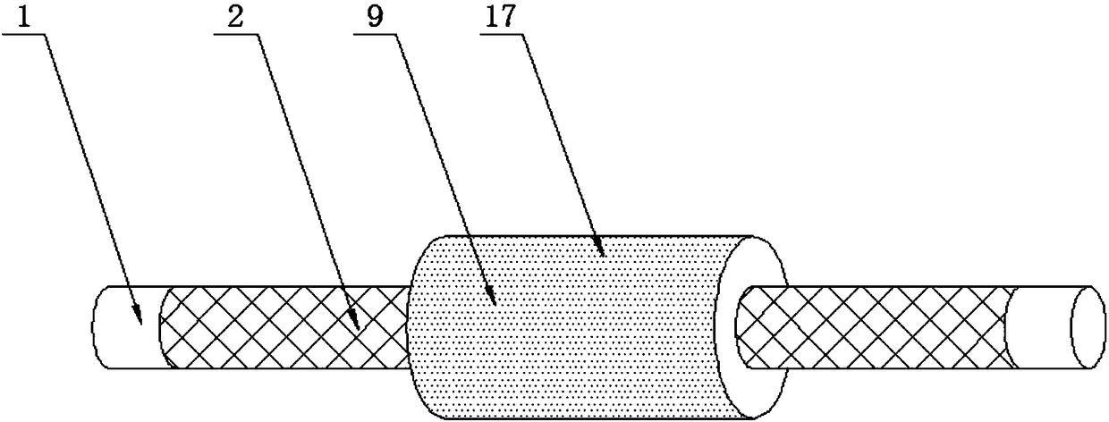
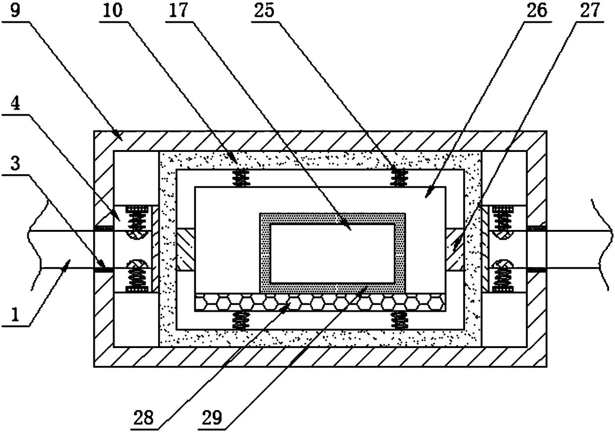
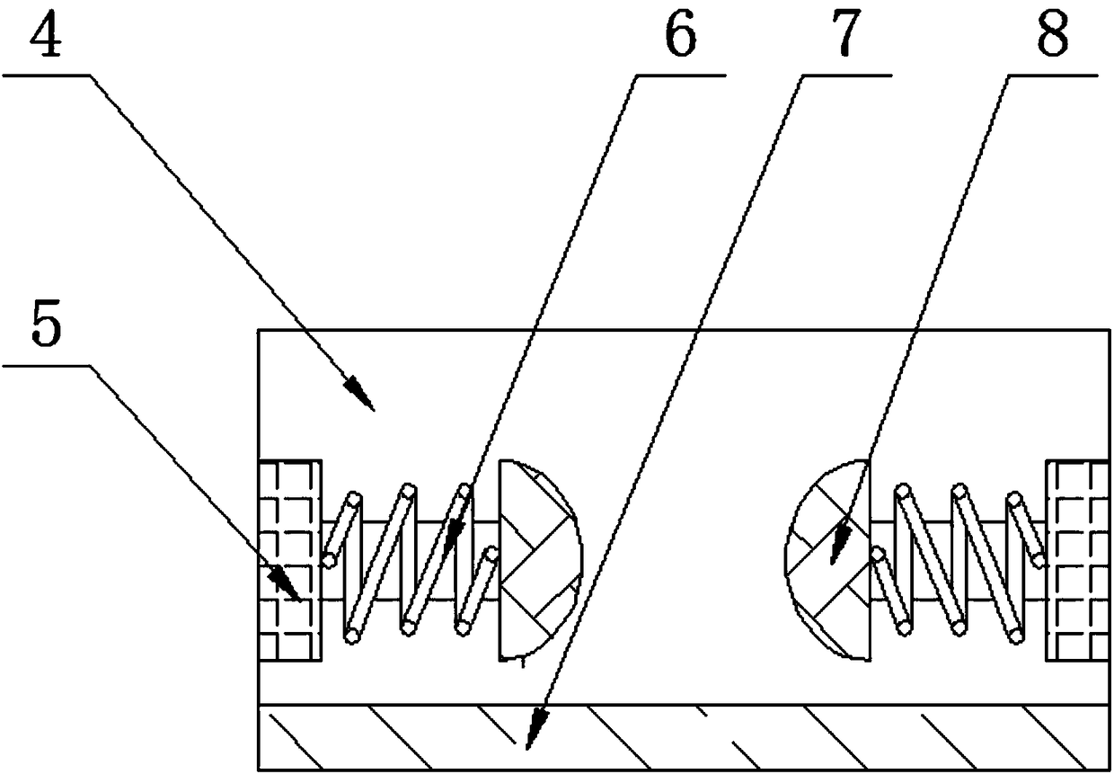
[0024] see Figure 1-5 , the present invention provides a gallium nitride light-emitting diode, including a pin 1, a dustproof cover 2, a sealing ring 3, a fixing seat 4, a bottom plate 5, a fastening spring 6, a baffle 7, a fixing block 8, and a package body 9 , protective cover 10, first ceramic layer 11, first antistatic layer 12, heat dissipation layer 13, waterproof layer 14, second antistatic layer 15, second ceramic layer 16, diode body 17, P-type elect...


PUM


Abstract

The invention discloses a gallium nitride light emitting diode and a preparation method thereof. The gallium nitride light emitting diode comprises pins, dustproof sleeves, sealing rings, a fixed base, bottom plates, fastening springs, a baffle, fixed clamping blocks, a packaging body, a protection sleeve, a first ceramic layer, a first anti-static layer, a heat dissipation layer, a waterproof layer, a second anti-static layer, a second ceramic layer, a diode body, a P type electrode, a GaN: Mg layer, an InGaN multi-quantum well, a GaN: Si layer, a GaN buffer layer, a sapphire substrate, an Ntype electrode, limiting springs, a mounting base, limiting blocks, a mounting partition plate and heat conducting adhesive; the pins are mounted on the two sides of the packaging body through the fixed base, and the outer sides of the pins are packaged with the dustproof sleeves; the baffle is mounted in the fixed base through a bolt; two bottom plates are mounted on the two sides of the top of the baffle through bolts; and the fastening springs are mounted on one sides of the bottom plates through buckles. The light emitting diode is convenient and quick to mount, stable in structure, has certain impact resistance and effectively improves use convenience.

Description

technical field [0001] The invention relates to the technical field of gallium nitride light emitting diodes, in particular to a gallium nitride light emitting diode and a preparation method thereof. Background technique [0002] Light emitting diode (light emitting diode) abbreviation and commonly known as LED is a semiconductor solid light emitting device; it uses a solid chip as a light emitting material, recombines through carriers in the semiconductor, and releases excess energy to cause photon emission, emitting red and yellow light. , blue, green, blue, orange, purple, white visible light or invisible light; the light-emitting diodes in the prior art have a complicated structure, complicated installation, and poor structural stability. When in use, the shock resistance is poor. At the same time, the prior art The light-emitting diodes in the present invention have high power consumption and low luminous brightness, which are far from meeting the needs of people. There...

Claims


Application Information

Patent Timeline
Patent Type & Authority Applications(China)
IPC IPC(8): H01L33/48H01L33/62H01L33/64H01L33/06H01L33/12H01L33/00
CPCH01L33/007H01L33/06H01L33/12H01L33/48H01L33/62H01L33/641H01L33/644H01L2933/0033H01L2933/0066H01L2933/0075
Inventor 王志敏黄丽凤
Owner RUGAO DACHANG ELECTRONICS
Why Eureka
Try Eureka