Preparation method of PCB (Printed Circuit Board) and PCB

A lamination plate and stepped groove technology, which is applied in the manufacture of printed circuits, printed circuits connected with non-printed electrical components, and the formation of electrical connection of printed components, can solve the problem of increasing signal loss, increasing the length of transmission lines, and increasing occupation. space and other issues, to achieve high-integrity transmission, reduce signal loss, and reduce occupied space.

Inactive Publication Date: 2018-09-28
DONGGUAN SHENGYI ELECTRONICS
View PDF5 Cites 7 Cited by
  • Summary
  • Abstract
  • Description
  • Claims
  • Application Information

AI Technical Summary

Problems solved by technology

However, this design makes the components can only be mounted or crimped on the surface of the PCB, which increases the occupied space of the PCB, which is not conducive to the realization of high-precision and high-integration assembly of the PCB, and in terms of function, when only connecting When connecting to one or several inner layers of the PCB, the existing design inevitably increases the length of the transmission line, increases signal loss, and causes signal distortion

Method used


Image

  • Preparation method of PCB (Printed Circuit Board) and PCB
  • Preparation method of PCB (Printed Circuit Board) and PCB
  • Preparation method of PCB (Printed Circuit Board) and PCB

Examples


Embodiment Construction

[0032] Embodiments of the present invention are described in detail below, and examples of the embodiments are shown in the drawings, wherein the same or similar reference numerals denote the same or similar elements or elements having the same or similar functions throughout. The embodiments described below by referring to the figures are exemplary and are intended to explain the present invention and should not be construed as limiting the present invention.

[0033] The technical solutions of the present invention will be further described below in conjunction with the accompanying drawings and through specific implementation methods.

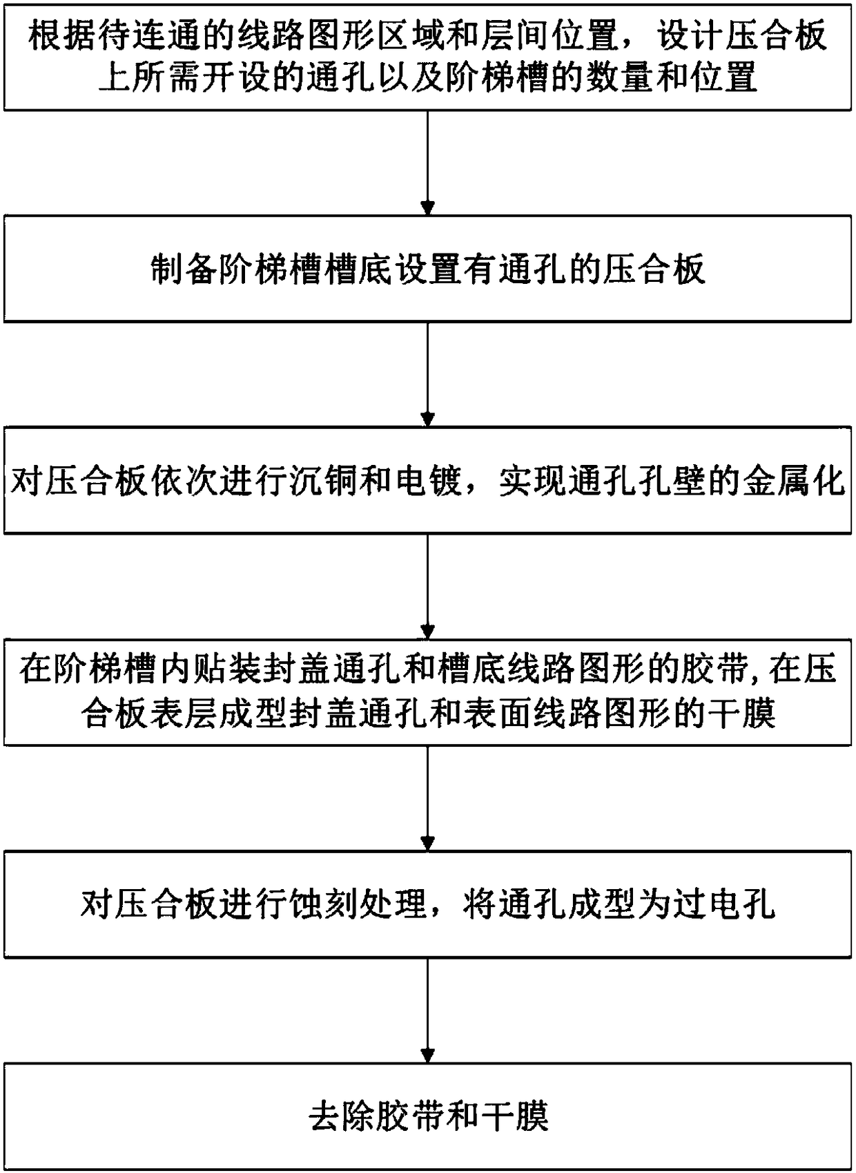
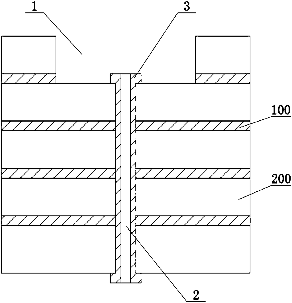
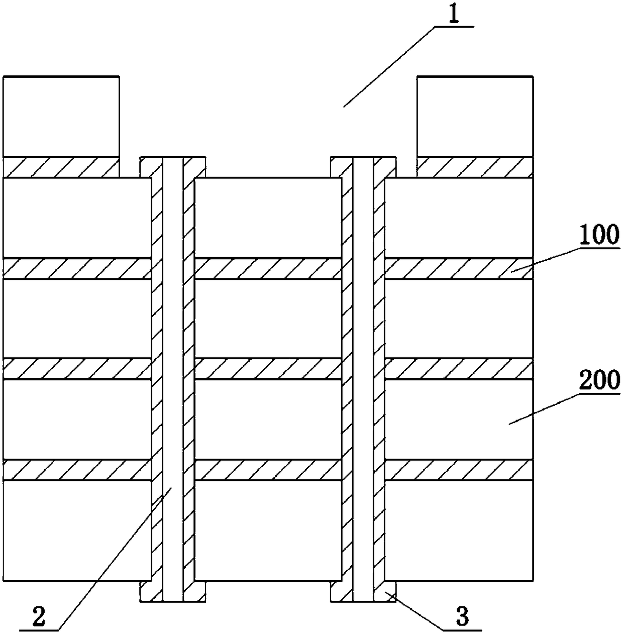
[0034] like Figure 1-Figure 5 As shown, the invention provides a method for preparing a PCB. The method comprises the steps of:

[0035] Step 1: Design the number and position of through holes 2 and stepped grooves 1 that need to be opened on the laminated board according to the graphic area of ​​the circuit to be connected and the positi...


PUM


Abstract

The invention belongs to the technical field of PCB (Printed Circuit Board) preparation and discloses a preparation method of a PCB and the PCB. The preparation method of the PCB includes the following steps: A, preparing a laminated plate which is provided with a through hole at a bottom of a step groove; B, performing copper deposition and electroplating on the laminated plate in sequence to implement metallization of a wall of the through hole; C, attaching an adhesive tape for covering the through hole in the step groove, and moulding a dry film for covering the through hole on a surface layer of the laminated plate; D, performing etching treatment on the laminated plate, and moulding the through hole into an electric transfer hole; and E, removing the adhesive tape and the dry film. The PCB is prepared with the preparation method of the PCB. According to the preparation method of the PCB and the PCB, a component can be installed in the non-metallic step groove on a sidewall safelyand reliably, so the occupation space of the PCB is effectively reduced; moreover, with the arrangement of the electric transfer hole in the step groove, a component mounted in the step groove by pressing can be directly connected to a one-layer or multi-layer circuit pattern on a specified copper layer at a lower side of the step groove, so the length of a transmission line is effectively shortened, the signal loss is reduced and the high-integrity transmission of a signal is implemented.

Description

technical field [0001] The invention relates to the technical field of PCB preparation, in particular to a method for preparing a PCB and the PCB. Background technique [0002] PCB (Printed Circuit Board), the Chinese name is printed circuit board, as a support for electronic components, it is an important electronic component. [0003] The interlayer circuit pattern realizes circuit connection through metallized holes, that is, network. In order to realize the design of different network wiring between layers, it is usually necessary to process multiple metallized holes, which seriously affects the wiring density and the efficiency of PCB processing and preparation. [0004] With the development of PCB towards dense and thin, the wiring density on PCB is getting higher and higher. In PCB design, in order to realize the connection and conduction of interlayer lines, it is generally realized by drilling holes at the places to be connected, and then metallizing the hole wall...

Claims


Application Information

Patent Timeline
Patent Type & Authority Applications(China)
IPC IPC(8): H05K1/18H05K3/42
CPCH05K1/183H05K3/429
Inventor 纪成光王洪府焦其正白永兰
Owner DONGGUAN SHENGYI ELECTRONICS
Why Eureka
Try Eureka