Novel electron emission device

A technology of electron emission and electron emission source, which is applied in the direction of electrical components, semiconductor devices, circuits, etc., can solve the problems of difficult realization, high hot carrier and lattice rate, and high material requirements, so as to reduce the difficulty of device technology, The effect of increasing device efficiency and improving space

Inactive Publication Date: 2018-10-02
南京合智电力科技有限公司
View PDF4 Cites 0 Cited by
  • Summary
  • Abstract
  • Description
  • Claims
  • Application Information

AI Technical Summary

Problems solved by technology

The rate of hot carriers and lattice heat balance is extremely high, so the requirements for materials are very high, and it is too difficult to realize

Method used


Image

  • Novel electron emission device

Examples


Embodiment Construction

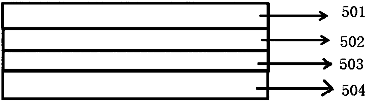
[0015] Such as figure 1 A novel electron-emitting device is shown, comprising a base substrate, a first electrode, a second electrode, and an electron emission source, which includes a first main electrode portion arranged on the surface of the base substrate and extending in a predetermined direction and extending from the first main electrode a first auxiliary electrode extending from the electrode portion; a second main electrode portion which is arranged on the surface of the base substrate and is separated from the first electrode and extends in a predetermined direction; and a second auxiliary electrode extending from the second main electrode portion. electrode; and it is arranged on at least one of the first and second electrodes, and a strengthening structure is also arranged between the electron emission source and the electrode, and the strengthening structure includes from top to bottom: A transparent conductive oxide layer 501 , a back surface field passivation la...


PUM


Abstract

The invention relates to a novel electron emission device, which comprises a base substrate, a first electrode, a second electrode and an electron emission source, wherein the first electrode comprises a first main electrode portion which is arranged on the surface of the base substrate and extends in a predetermined direction and a first auxiliary electrode extending from the first main electrodeportion; the second electrode comprises a second main electrode portion which is arranged on the surface of the base substrate, is isolated from the first electrode and extends in a predetermined direction and a second auxiliary electrode extending from the second main electrode portion; and the electron emission source is arranged at least one of the first electrode and the second electrode, theelectron emission source and the electrode are further provided with an enhancement structure therebetween, the enhancement structure sequentially comprises a first transparent conductive oxide layer, a back surface field passivation layer used for reducing carrier recombination, a second transparent conductive oxide layer and a high-conductivity high-heat-insulation semiconductor material layerfrom top to bottom. The novel electron emission device has the advantages of simple structure, easy manufacturing, practicability and efficiency.

Description

technical field [0001] The invention relates to the technical field of electronic equipment, in particular to a novel electron emitting device. Background technique [0002] At present, the energy loss caused by the mismatch between the energy band structure of the absorbing layer material and the solar spectrum in conventional photovoltaic cell devices accounts for about 50% of the overall spectral energy, and this part of the lost energy is eventually dissipated in the form of heat. Technologies such as split-spectrum photovoltaic cells and multi-junction solar cells reduce this loss by improving the matching degree of the energy band structure of the absorbing layer with the solar spectrum. However, the cost of multi-cell photovoltaic cells with split-spectrum photovoltaic cells is extremely high, and the device design and process are difficult, so it is difficult to promote in a large area. The hot carrier battery proposed in recent years can theoretically achieve a hig...

Claims


Application Information

Patent Timeline
Patent Type & Authority Applications(China)
IPC IPC(8): H01L31/0525H01L31/07
CPCH01L31/0547H01L31/07Y02E10/52
Inventor 冯亚东朱继红李秋华陈勇
Owner 南京合智电力科技有限公司
Why Eureka
Try Eureka