

Antenna and fabrication method thereof
An antenna and microstrip line technology, applied in the direction of antennas, resonant antennas, antenna arrays, etc., can solve the problems of integrated electronic chips or passive components that are difficult to combine with glass, and glass cannot be drilled and connected.
- Summary
- Abstract
- Description
- Claims
- Application Information
AI Technical Summary
Problems solved by technology
Method used
Image

Examples
Embodiment 1
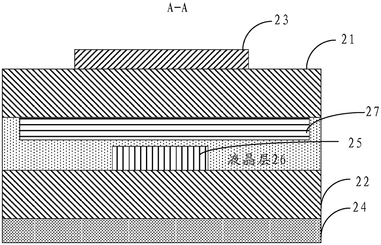
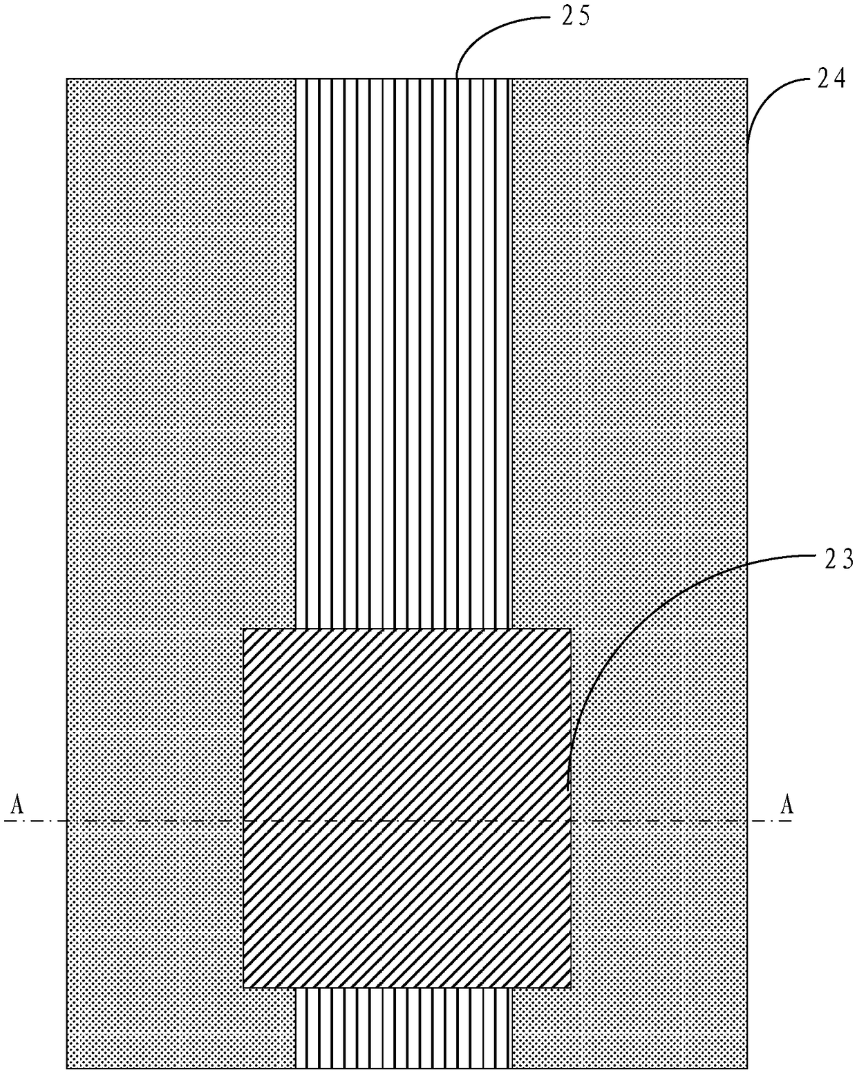
[0064] refer to Figure 5 As shown, this embodiment provides an antenna, including:
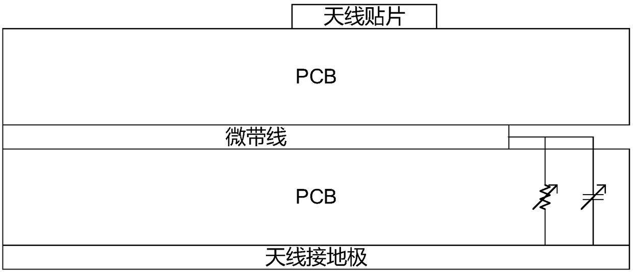
[0065] The first substrate 51 and the second substrate 52 opposite to each other; the first antenna electrode 53 arranged on the side of the first substrate 51 away from the second substrate 52; the second antenna arranged on the side of the second substrate 52 away from the first substrate 51 The electrode 54 and the microstrip line 55 arranged on the side of the second substrate 52 close to the first substrate 51; E in the figure is a schematic illustration of the edge electric field lines of the microstrip line;
[0066] It should be noted that the fringe electric field of the microstrip line will not affect the control of the liquid crystal layer by the driving electrode assembly in the embodiment of the present invention, because compared with the voltage required to normally control the deflection of liquid crystal molecules in the liquid crystal layer, the microstrip line The voltage ...
Embodiment 2
[0077] refer to Figure 8 As shown, this embodiment provides an antenna, including:
[0078] The first substrate 81 and the second substrate 82 facing each other; the first antenna electrode 83 arranged on the side of the first substrate 81 away from the second substrate 82; the second antenna arranged on the side of the second substrate 82 away from the first substrate 81 The electrode 84 and the microstrip line 85 arranged on the side of the second substrate 82 close to the first substrate 81; E in the figure is a schematic diagram of the edge electric field lines of the microstrip line;
[0079] A liquid crystal layer 86 disposed between the first substrate 81 and the second substrate 82; the initial alignment of the liquid crystal layer includes vertically aligned liquid crystals, Figure 8 The ellipses in the figure represent liquid crystal molecules;
[0080] The orthographic projection of the first antenna electrode 83 on the second substrate 82 and the orthographic p...
Embodiment 3
[0089] refer to Figure 10 As shown, this embodiment provides an antenna, including:
[0090] The first substrate 101 and the second substrate 102 facing each other; the first antenna electrode 103 arranged on the side of the first substrate 101 away from the second substrate 102; the second antenna arranged on the side of the second substrate 102 away from the first substrate 101 The electrode 104 and the microstrip line 105 arranged on the side of the second substrate 102 close to the first substrate 101; E in the figure is a schematic diagram of the edge electric field lines of the microstrip line;
[0091] A liquid crystal layer 106 disposed between the first substrate 101 and the second substrate 102; the initial alignment of the liquid crystal layer includes horizontally aligned liquid crystals, Figure 10 The ellipses in the figure represent liquid crystal molecules;
[0092] The orthographic projection of the first antenna electrode 103 on the second substrate 102 an...
PUM
| Property | Measurement | Unit |
|---|---|---|
| Thickness | aaaaa | aaaaa |
Abstract
Description
Claims
Application Information