Semiconductor packaging structure and manufacturing method thereof

A technology of packaging structure and manufacturing method, which is applied in the direction of semiconductor/solid-state device manufacturing, semiconductor devices, semiconductor/solid-state device parts, etc., can solve the problems of affecting the results and difficult control of etching depth, so as to simplify the process, improve production efficiency and The effect of yield

Inactive Publication Date: 2018-10-09
POWERTECH TECHNOLOGY
View PDF4 Cites 0 Cited by
  • Summary
  • Abstract
  • Description
  • Claims
  • Application Information

AI Technical Summary

Problems solved by technology

However, in the above manufacturing process, the etching depth when removing the first conductive metal is n

Method used


Image

  • Semiconductor packaging structure and manufacturing method thereof
  • Semiconductor packaging structure and manufacturing method thereof
  • Semiconductor packaging structure and manufacturing method thereof

Examples


Embodiment Construction

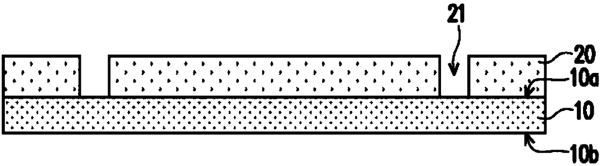
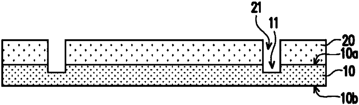
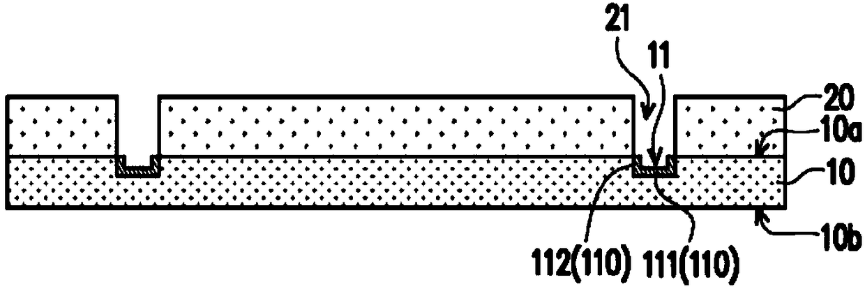
[0041] Figure 1A to Figure 1I is a schematic cross-sectional view of the manufacturing process of the semiconductor package structure according to an embodiment of the present invention. The manufacturing method of the semiconductor package structure 100 of the present embodiment comprises the following steps: first, please refer to Figure 1A , providing a substrate 10, wherein the substrate 10 has a first surface 10a and a second surface 10b opposite to each other. Next, a mask layer 20 is formed on the first surface 10a of the substrate 10, wherein the mask layer 20 has a plurality of openings 21, and these openings 21 expose part of the first surface 10a, and the shape of these openings can be circular or square, but the invention is not limited thereto. In this embodiment, the material of the substrate 10 may be copper or other conductive metals.

[0042] On the other hand, the mask layer 20 may be a patterned photoresist layer formed by a photolithography process. As ...


PUM


Abstract

The present invention provides a semiconductor packaging structure including a circuit board, at least one chip, and a packaging layer. The circuit board includes a dielectric layer, a plurality of conductive pillars, a circuit layer, and a plurality of protective layers. The conductive pillars extend through the dielectric layer. Each of the conductive pillars has opposing first and second end portions. The second end portion protrudes from the dielectric layer. The circuit layer is disposed on the dielectric layer. The circuit layer is connected to the first end portion. The protective layers coat the second end portions of the conductive pillars. The material of the protective layers is different from the material of the conductive pillars. The chip is disposed on the dielectric layer.The chip and the circuit layer are located on the same side of the dielectric layer. The chip is electrically connected to the circuit layer. The packaging layer is disposed on the dielectric layer and coats the chip. A method for manufacturing the semiconductor packaging structure is also provided.

Description

technical field [0001] The invention relates to a packaging structure and a manufacturing method thereof, in particular to a semiconductor packaging structure and a manufacturing method thereof. Background technique [0002] With the advancement of technology, the size of electronic products launched on the market is also continuously reduced, and is developing towards the trend of being thin, light, small and easy to carry. In order to meet the development trend of thinner and lighter electronic products, the size of semiconductor packaging structures disposed in electronic products is also continuously reduced. [0003] In the prior art, the packaging substrate of the semiconductor packaging structure is composed of a core layer and circuit layers arranged symmetrically on opposite sides of the core layer. Therefore, a semiconductor package structure without a core layer (coreless) is proposed, and its manufacturing steps are as follows: First, a first conductive metal la...

Claims


Application Information

Patent Timeline
IPC IPC(8): H01L21/56H01L21/60H01L23/498H01L23/31
CPCH01L2224/32225H01L2224/48227H01L2224/73265H01L2924/181H01L2924/00012H01L2924/00H01L21/568H01L23/3107H01L23/3121H01L23/49827H01L24/85
Inventor 张连家蓝源富柯志明
Owner POWERTECH TECHNOLOGY
Why Eureka
Try Eureka