Array substrate, preparation method and application thereof and performance improvement method

A technology for array substrates and base substrates, which is applied in the field of array substrates and its preparation, can solve problems such as uncontrollable electric field strength of additional electric field, warpage in the saturation region of the output characteristic curve, and in-depth research on array substrates, etc.

Active Publication Date: 2018-10-09
BOE TECH GRP CO LTD
View PDF5 Cites 8 Cited by
  • Summary
  • Abstract
  • Description
  • Claims
  • Application Information

AI Technical Summary

Problems solved by technology

[0002] In the manufacturing process of display panels or array substrates, the bottom blocking metal (BSM) layer is often used for light shielding layer, fingerprint identification, or in flexible display panels, it is also used to eliminate the influence of mobile charges on the flexible substrate side, but because BSM does not Connected to the circuit, the electric field strength of the addi

Method used


Image

  • Array substrate, preparation method and application thereof and performance improvement method
  • Array substrate, preparation method and application thereof and performance improvement method
  • Array substrate, preparation method and application thereof and performance improvement method

Examples


Example Embodiment

[0035] The embodiments of the present invention are described in detail below. The embodiments described below are exemplary, and are only used to explain the present invention, but should not be construed as limiting the present invention. Where specific techniques or conditions are not indicated in the embodiments, the procedures shall be carried out in accordance with the techniques or conditions described in the literature in the field or in accordance with the product specification. The reagents or instruments used without the manufacturer's indication are all conventional products that are commercially available.

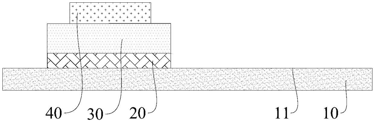
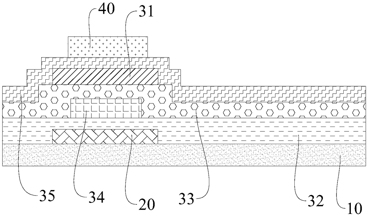
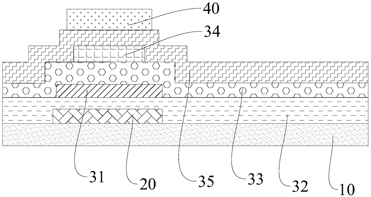
[0036] In one aspect of the present invention, the present invention provides an array substrate. According to an embodiment of the present invention, refer to Figure 1-4 , The array substrate includes: a base substrate 10; a shielding layer 20, the shielding layer 20 is provided on one surface 11 of the base substrate 10; a thin film transistor 30, the thin fi...


PUM

PropertyMeasurementUnit
Thicknessaaaaaaaaaa

Abstract

The invention provides an array substrate, a preparation method and an application thereof and a performance improvement method. The array substrate comprises a substrate, a shielding layer, a thin film transistor and a compensation layer, wherein the shielding layer is arranged on one surface of the substrate; the thin film transistor is arranged on the substrate and covers the shielding layer; and the compensation layer is arranged on one side, far from the substrate, of the thin film transistor and used for forming a second electric field in an active layer of the thin film transistor. Therefore, by changing the electric field distribution in the active layer of the thin film transistor, influence of the first electric field to the characteristic of the thin film transistor can be compensated, so that a technical effect of improving or eliminating an abnormal phenomenon of output characteristic curved saturation region warping can be realized, and current normal output can be ensured; and meanwhile, the adverse influence caused by change of a threshold voltage of the thin film transistor due to the first electric field can be improved and compensated, the problem of threshold voltage drifting and the like can be solved, and the thin film transistor can recover to the working state when the active layer is not influenced by the first electric field, and even a higher level.

Description

technical field [0001] The present invention relates to the field of display technology, in particular, to an array substrate and its preparation method, application and performance improvement method. Background technique [0002] In the manufacturing process of display panels or array substrates, the bottom blocking metal (BSM) layer is often used for light shielding layer, fingerprint identification, or in flexible display panels, it is also used to eliminate the influence of mobile charges on the flexible substrate side, but because BSM does not Connected to the circuit, the electric field strength of the additional electric field formed by it is uncontrollable. When the additional electric field acts on the active layer, it may cause the abnormal phenomenon of warping in the saturation area of ​​the output characteristic curve, making the output current abnormal, and even affecting the thin film transistor. threshold voltage. [0003] Therefore, the research on the arr...

Claims


Application Information

Patent Timeline
IPC IPC(8): H01L23/58H01L27/12H01L21/84
CPCH01L23/585H01L27/1218H01L27/1296H01L29/78633H01L27/1251H01L27/127
Inventor 刘政赵梦田宏伟
Owner BOE TECH GRP CO LTD
Why Eureka
Try Eureka