A TFT LCD array base plate and the manufacturing method thereof

A manufacturing method and array substrate technology, applied in semiconductor/solid-state device manufacturing, optics, instruments, etc., can solve the problems of reduced aperture ratio and increased cost, and achieve the effect of reducing the resistance of data lines

Active Publication Date: 2009-03-04
BEIJING BOE OPTOELECTRONCIS TECH CO LTD +1
View PDF3 Cites 0 Cited by
  • Summary
  • Abstract
  • Description
  • Claims
  • Application Information

AI Technical Summary

Problems solved by technology

However, the method of using composite film to increase film thickness and line width often brings about disadvantages such as increased cost and reduced aperture ratio.

Method used


Image

  • A TFT LCD array base plate and the manufacturing method thereof
  • A TFT LCD array base plate and the manufacturing method thereof
  • A TFT LCD array base plate and the manufacturing method thereof

Examples


Embodiment Construction

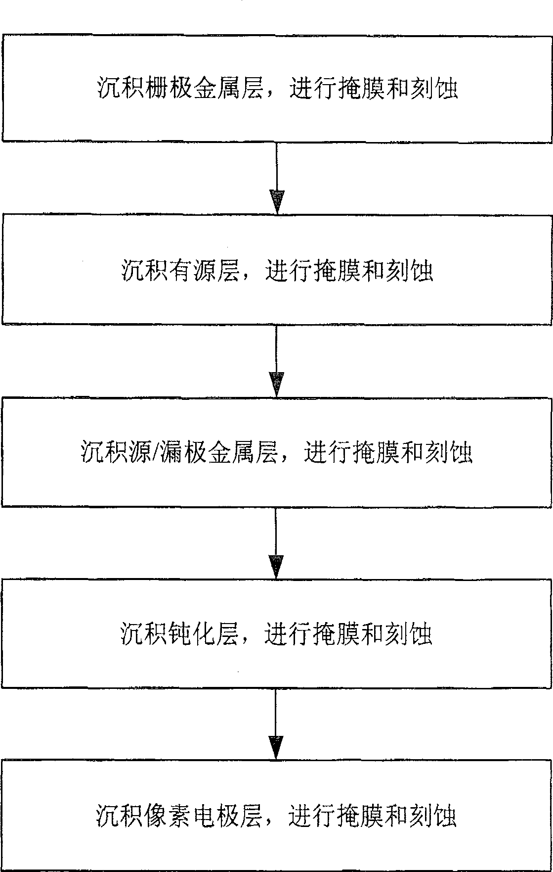
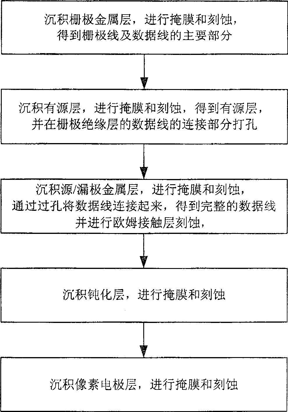
[0035] Such as image 3 Shown, be that the flowchart of the present invention comprises the following steps:

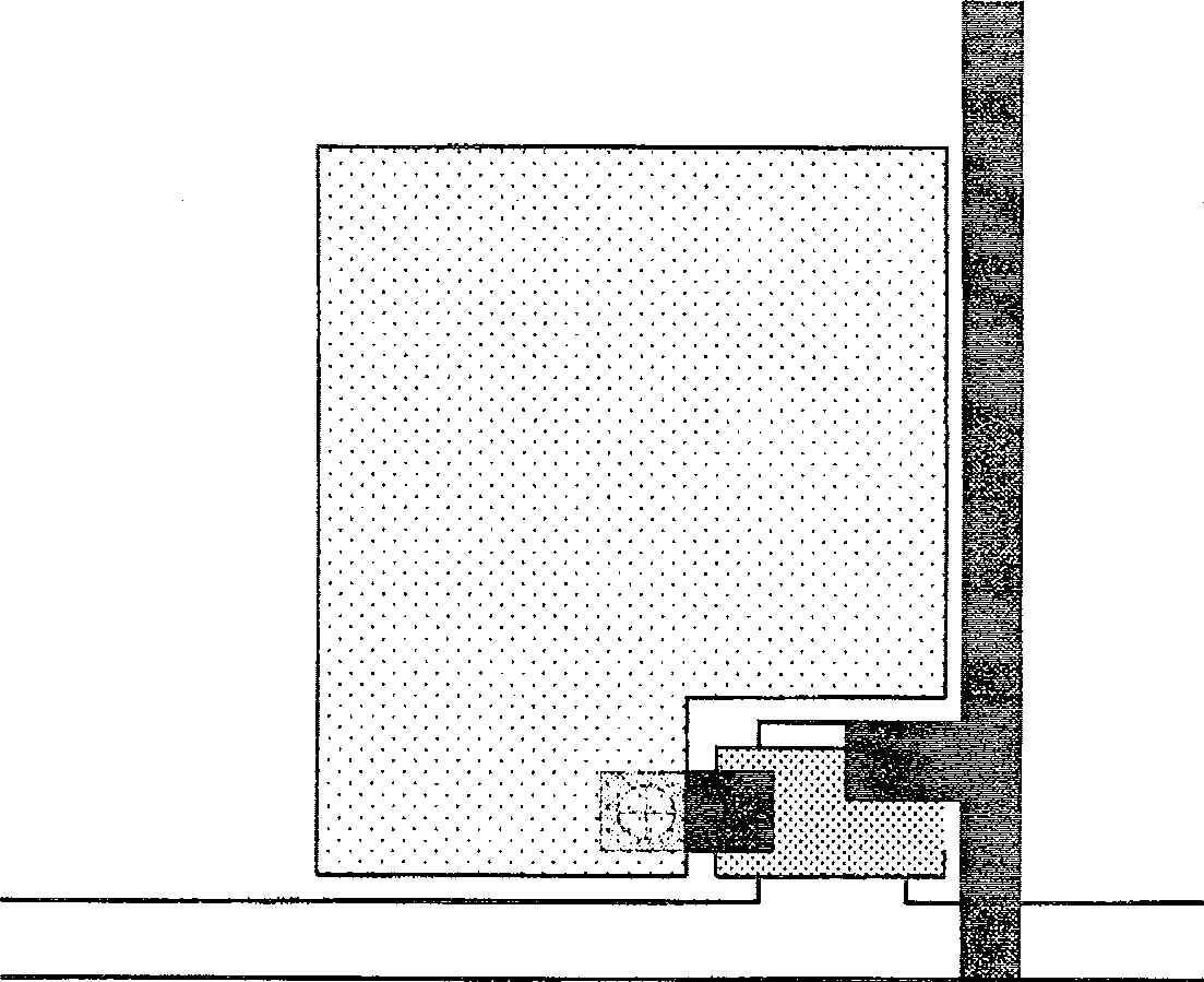
[0036] Step 1. First deposit Gate metal on a clean glass substrate (Bare Glass) by sputtering. Gate metal is a composite film composed of one of AlNd, Al, Cu, Mo, MoW or Cr or any combination of deposition layers. , for example: Mo / AlNd / Mo composite film, AlNd / Mo composite film; then, carry out Gate photolithography, after etching process, get such as Figure 4 The structure shown, along the A-A section as Figure 5 As shown, the gate line and the gate electrode 2, and the main part 3 of the data line are obtained.

[0037]Step 2: Deposit multilayers (MultiLayer) on the substrate formed in step 1 by using chemical vapor phase (PECVD), including one or more insulating dielectric layers such as SiNx, SiOx, SiOxNy, etc., and a-Si active layer and ohmic contact Layer, gray tone active layer mask (G / T Act.Mask) is carried out by using Gray Tone technology, the active la...


PUM


Abstract

The related TFT LCD array substrate comprises: a glass substrate with grid wire and grid electrode, an insulation medium layer on the electrode, a semi-conductor layer, an ohmic contact layer, a transparent pixel electrode, a source / drain electrode, a sectional data line including the primary and connection parts, and a passive layer, wherein the primary part of data line is formed in the same photo etching as the grid line and electrode. Compared with 5Mask technique, this invention can reduce data line resistance, and eliminates the data signal RC-delay effect.

Description

technical field [0001] The invention relates to a TFT LCD array substrate and a manufacturing method thereof, in particular to a TFT LCD array substrate capable of effectively reducing the resistance of data lines and a manufacturing method of the substrate. Background technique [0002] The liquid crystal display represented by Thin Film Transistor Liquid Crystal Display (TFT LCD for short) has become an important flat panel display mode. [0003] The manufacturing technology of the TFT LCD array substrate has gone through the development process from the 7th photolithography technology (7Mask) to the current 5th photolithography technology (5Mask). The 5Mask technology has become the main manufacturing method of the current TFT LCD array substrate, including the gate electrode Photolithography (Gate Mask), active layer photolithography (ActiveMask), source and drain electrode photolithography (S / D Mask), via hole photolithography (Via Hole Mask) and pixel electrode layer p...

Claims


Application Information

Patent Timeline
Patent Type & Authority Patents(China)
IPC IPC(8): H01L27/12H01L23/52H01L21/84H01L21/768G02F1/136G02F1/1345
CPCH01L27/124
Inventor 邓朝勇林承武
Owner BEIJING BOE OPTOELECTRONCIS TECH CO LTD
Why Eureka
Try Eureka