
IC wafer surface defect detection method

A defect detection and wafer technology, applied in image data processing, instruments, calculations, etc., can solve the problems of cumbersome processing steps, large amount of image data, high computer hardware requirements, etc., and achieve the effect of fast and effective detection and simple algorithm

Inactive Publication Date: 2018-10-12
北京京仪仪器仪表研究总院有限公司
View PDF4 Cites 27 Cited by
  • Summary
  • Abstract
  • Description
  • Claims
  • Application Information

AI Technical Summary

Problems solved by technology

The amount of image data collected by this method is large, the processing steps are cumbersome, and the hardware requirements of the computer are relatively high.

Method used


Image

  • IC wafer surface defect detection method
  • IC wafer surface defect detection method

Examples


Embodiment Construction

[0051] In order to make the object, technical solution and advantages of the present invention more clear, the present invention will be further described in detail below in conjunction with the accompanying drawings. However, it should be understood that the specific examples are provided only for better understanding of the present invention, and they should not be construed as limiting the present invention.

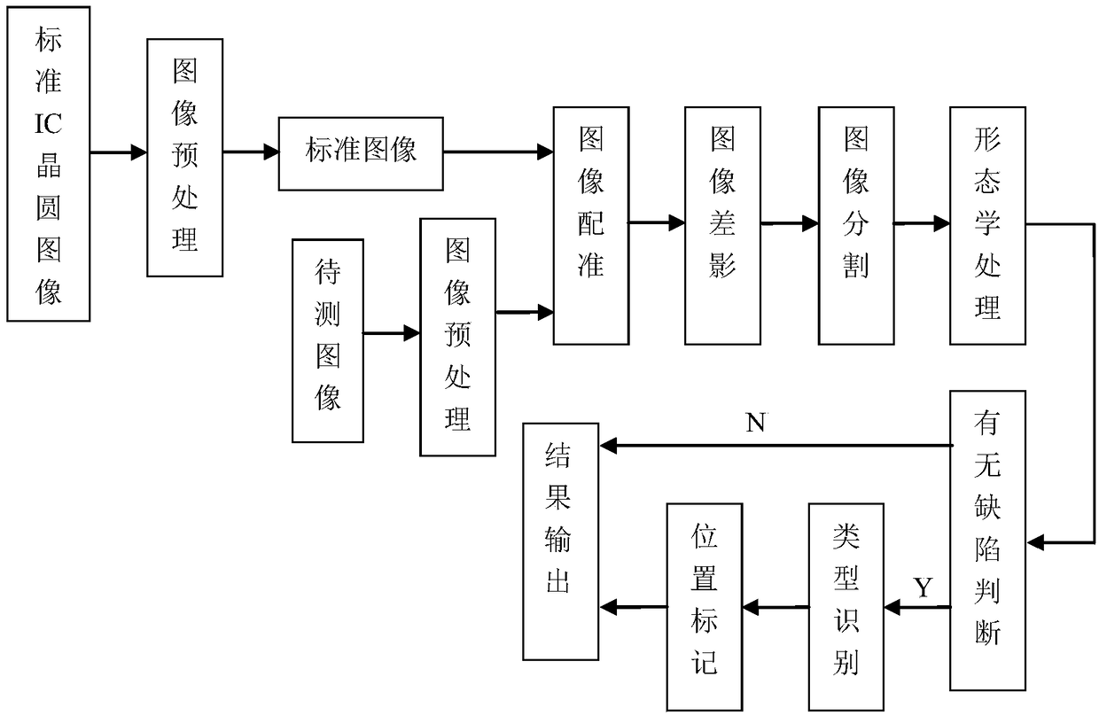
[0052] like figure 1 Shown is a schematic flow chart of the IC wafer surface defect detection method involved in the present invention. Specific steps are as follows:

[0053] The image of the standard wafer is acquired by a white light interferometer, and the standard image is histogram equalized to improve the image contrast, followed by a median filter to filter out the noise and smooth the image, and then stored in the standard image sample library. Then, the original image of a single structural unit on the surface of the wafer to be inspected is obtained by a ...


PUM


Abstract

The invention belongs to the technical field of the wafer detection, and especially relates to an IC wafer surface defect detection method for a product with a repeated pattern array structure. The method comprises the following steps: a, acquiring a standard IC wafer image through a white light interferometer, performing image pre-processing on the standard IC wafer image, and storing the same ina standard image sample base, and then acquiring an original image of a to-be-detected IC wafer surface single structure unit through the white light interferometer, namely, the to-be-detected image,and performing the image pre-processing; b, performing image registration on the standard image of the standard image sample base and the to-be-detected image after the image pre-processing; c, orderly performing gray difference computation, image binarization processing and morphological method processing on the standard image and the registered to-be-detected image to obtain a defect image; andd, performing defect type identification and defect location identification on the defect image. Through the detection method disclosed by the invention, the IC wafer surface defect detection is realized under the condition that the wafer surface has the repeated pattern array, and the method has the features of being simple in algorithm and fast and effective in detection.

Description

Technical field [0001] The invention belongs to the field of wafer detection technology, and in particular relates to a method for detecting surface defects of IC (integrated circuit, integrated circuit) wafers for products with repeating pattern array structures. Background technique [0002] In the semiconductor industry, defect detection on wafer surfaces generally requires high efficiency and accuracy, and the ability to capture defects quickly and effectively. For the detection of wafer surface defects, microscope visual inspection was mainly used at first. With the development of technology, the semiconductor process has developed from 90nm to 14nm. Visual inspection of pattern defects can no longer meet the current demand for accuracy. There are more and more data characterizing wafer surface defects, and inspections rely on manual labor. It has become increasingly beyond its capabilities. [0003] Currently, the most widely used wafer surface defect detection metho...

Claims


Application Information

Patent Timeline
IPC IPC(8): G06T7/00G06T7/136G06T7/33G06T5/40
CPCG06T5/40G06T7/001G06T7/136G06T7/33G06T2207/20032G06T2207/30148
Inventor 刘西锋胡玉薇
Owner 北京京仪仪器仪表研究总院有限公司
Features
  • Generate Ideas
  • Intellectual Property
  • Life Sciences
  • Materials
  • Tech Scout
  • Unparalleled Data Quality
  • Higher Quality Content
  • 60% Fewer Hallucinations
Learn More