Sensitive amplifier, semiconductor storage device and voltage difference amplification method

A technology of sense amplifier and voltage difference, applied in the field of semiconductor storage device and voltage difference amplification, sense amplifier field, to achieve the effect of increasing sensitivity and improving amplification speed

Pending Publication Date: 2018-10-12
CHANGXIN MEMORY TECH INC
View PDF7 Cites 2 Cited by
  • Summary
  • Abstract
  • Description
  • Claims
  • Application Information

AI Technical Summary

Problems solved by technology

[0005] Embodiments of the present invention provide a sensitive amplifier, a semiconductor storage device, and a voltage difference amplification method to solve or alleviate one or more technical problems in the prior art

Method used


Image

  • Sensitive amplifier, semiconductor storage device and voltage difference amplification method
  • Sensitive amplifier, semiconductor storage device and voltage difference amplification method
  • Sensitive amplifier, semiconductor storage device and voltage difference amplification method

Examples


Embodiment Construction

[0053] In the following, only some exemplary embodiments are briefly described. As those skilled in the art would realize, the described embodiments may be modified in various different ways, all without departing from the spirit or scope of the present invention. Accordingly, the drawings and descriptions are to be regarded as illustrative in nature and not restrictive.

[0054]In the description of the present invention, it should be understood that the terms "first" and "second" are used for description purposes only, and cannot be interpreted as indicating or implying relative importance or implicitly indicating the quantity of indicated technical features. Thus, a feature defined as "first" and "second" may explicitly or implicitly include one or more of these features. In the description of the present invention, "plurality" means two or more, unless otherwise specifically defined.

[0055] In the present invention, unless otherwise clearly specified and limited, terms...


PUM


Abstract

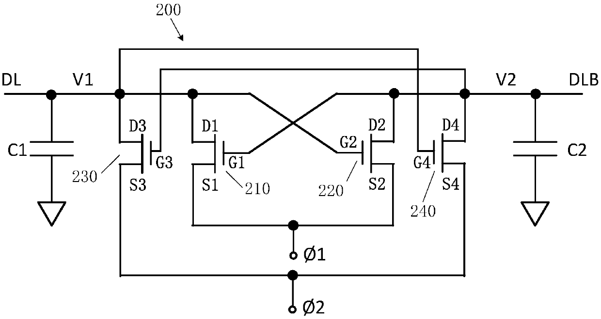
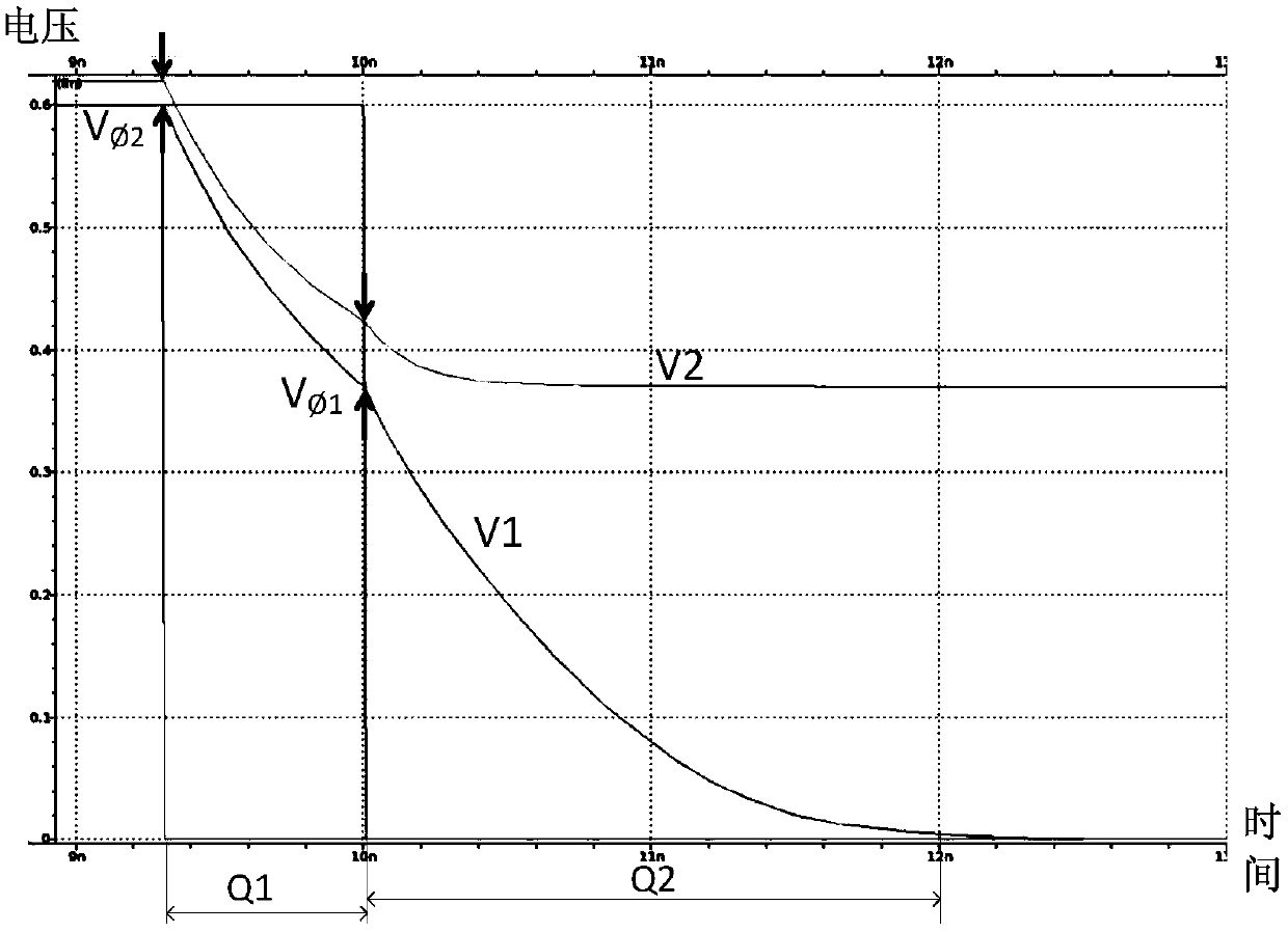
The invention provides a sensitive amplifier, a semiconductor storage device and a voltage difference amplification method. The sensitive amplifier comprises four transistors, wherein the drain electrode of the first transistor is connected with a first data line, a source electrode is connected with a first clock signal, and a grid element is connected with a second data line; the drain electrodeof the second transistor is connected with the second data line, the source electrode is connected with a first clock signal, and the grid electrode is connected with the first data line; the sourceelectrode of the third transistor is connected with a second clock signal, and the grid electrode is connected with the second data line; the drain electrode of the fourth transistor is connected withthe second data line, the source electrode is connected with the second clock signal, and the grid electrode I connected with the first data line; the second clock signal is started when a voltage difference between on the first data line and voltage on the second data line achieves a first threshold value, and the third transistor and the fourth transistor amplify the voltage difference; and thefirst clock signal is started when the voltage difference achieves a second threshold value, so that the first transistor pulls down voltage on the first data line, flexibility can be improved, and amplification speed is improved.

Description

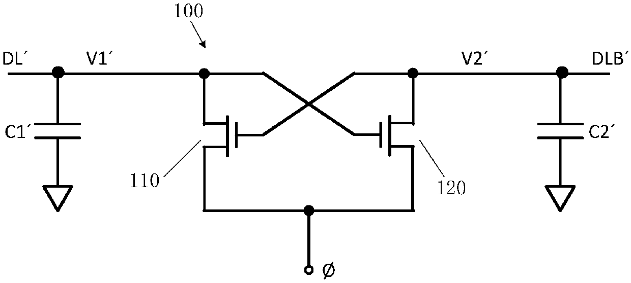
technical field [0001] The invention relates to the technical field of semiconductor storage, in particular to a sensitive amplifier, a semiconductor storage device and a voltage difference amplification method. Background technique [0002] Semiconductor storage devices, such as Static Random-Access Memory (SRAM for short), Dynamic Random-Access Memory (Dynamic Random Access Memory, DRAM for short), Read-Only Memory (ROM for short), flash memory etc., usually a two-dimensional array composed of memory cells (Memory Cell). The memory cells of each row can be selected by a word line (Word Line, referred to as WL), and the memory cells of each column can be selected by a bit line (Bit Line, referred to as BL) and a reverse bit line (Bit Line Bar, referred to as BLB). To write information into memory cells or to read stored information from memory cells. [0003] Reading information from a storage unit or writing information to a storage unit can be performed by a two-stage s...

Claims


Application Information

Patent Timeline
Patent Type & Authority Applications(China)
IPC IPC(8): G11C7/06G11C7/08
CPCG11C7/062G11C7/08
Inventor 不公告发明人
Owner CHANGXIN MEMORY TECH INC
Why Eureka
Try Eureka