Contact type semiconductor material test head

A material testing and semiconductor technology, applied in single semiconductor device testing, semiconductor characterization, electrical measurement, etc., can solve the problems that the probe pressure reproducibility cannot achieve high precision, it is difficult to reduce the probe spacing, and affect the test results, etc. Achieve the effects of stable and reliable probe force, high probe pressure accuracy, and no sluggish zone

Active Publication Date: 2018-10-16
SHIPELE CO LTD
View PDF13 Cites 0 Cited by
  • Summary
  • Abstract
  • Description
  • Claims
  • Application Information

AI Technical Summary

Problems solved by technology

The lateral force caused by this type of structure causes the probe to form additional friction in the guide bearing. This friction will have a discrete impact on the accuracy of the pressure due to reasons such as material and manufacturing, so that the probe and the measured There is uncertainty interference in the actual contact pressure of the surface, and the upper and lower envelopes of the pressure have a large area, so that the probe pressure reproducibility cannot achieve high accuracy whether it is static or dynamic, thus affecting the test results.
However, using the helical compression spring to directly apply force to the probe has difficulties in structural layout; if the pressure of the probe is directly adjusted, it will be difficult to reduce the distance between the probes, so it is rarely used in the field of semiconductor testing.

Method used


Image

  • Contact type semiconductor material test head
  • Contact type semiconductor material test head
  • Contact type semiconductor material test head

Examples


Embodiment Construction

[0027] In order to make the purpose, technical solutions and advantages of the present invention more clear, the present invention will be further described in detail below in conjunction with specific examples. It should be understood that these descriptions are exemplary only, and are not intended to limit the scope of the present invention. Also, in the following description, descriptions of well-known structures and techniques are omitted to avoid unnecessarily obscuring the concept of the present invention.

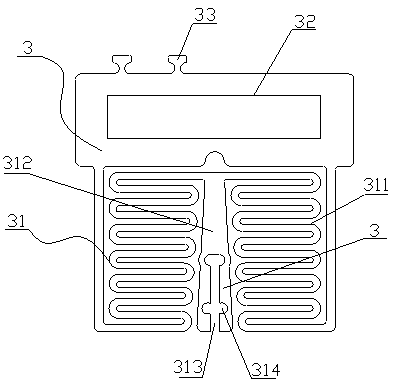
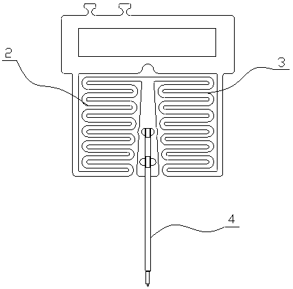
[0028] A contact type semiconductor material testing head comprises a housing 1 and a probe assembly 2 arranged in the housing 1 .

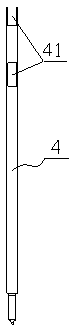
[0029] The probe assembly 2 includes a flat extension spring 3 and a probe 4, and the flat extension spring 3 is bilaterally symmetrical, and the flat extension spring 3 includes a lower spring end 31 and an upper extension end 32, and the extension end 32 The spring end 31 includes spring parts 311 on both sides and a middle part 312 ...


PUM


Abstract

The invention discloses a contact type semiconductor material test head which comprises a shell and a probe combination arranged in the shell; wherein the probe combination comprises flat tension spring sand probes; and the two sides of each flat tension spring are symmetric. Each flat tension spring comprises a spring end at the lower part and an extending end at the upper part, the probe is fixed at the center of the spring end, and the extending end is in a hollow flat plate shape. A plurality of flat tension springs are overlapped together and arranged in the shell through the extending ends, the spring ends of the flat tension springs are arranged at the lower part of the shell, and an insulating film isolation layer is arranged between every two adjacent flat tension springs. The spring end of each flat tension spring comprises spring parts arranged on the two sides and a middle part arranged between the two spring parts, a vertical clamping groove is formed in the center of themiddle part, and the probe is arranged in a vertical clamping groove arranged in the center of the middle part. According to the invention, the lateral force is completely eliminated, the structure issimple, the number of parts is small, and the distance between the probes can be greatly reduced. The negative influence on the overall test precision caused by the edge effect in the test is reduced, the test precision is high, the cost is low, and the service life is long.

Description

technical field [0001] The invention relates to the technical field of semiconductor material testing, in particular to a contact type semiconductor material testing head with simple structure, high testing precision, small probe spacing, low cost and long service life. Background technique [0002] Existing contact type semiconductor test head, in addition to being arranged with electric circuit inside, mainly is constituted the factor condition of test head by probe and spring. Due to the small spacing between the probes of the semiconductor test head and the limited space for arranging the corresponding mechanisms, generally a cantilever compression spring is used to apply force to the probes, or a lever is extended to indirectly apply force to the probes. The lateral force caused by this type of structure causes the probe to form additional friction in the guide bearing. This friction will have a discrete impact on the accuracy of the pressure due to reasons such as mate...

Claims


Application Information

Patent Timeline
IPC IPC(8): G01R1/073
CPCG01R1/0735G01R1/07357G01R31/2601G01R31/2648
Inventor 胡谱金胡中元
Owner SHIPELE CO LTD
Why Eureka
Try Eureka