A Method for Improving Control Gate Filling Defects

A technology for controlling gates and defects, applied in semiconductor devices, electrical components, circuits, etc., can solve problems such as reducing carrier mobility, reducing polysilicon grain boundaries, and increasing polysilicon resistance.

Active Publication Date: 2021-04-02
WUHAN XINXIN SEMICON MFG CO LTD
View PDF4 Cites 0 Cited by
  • Summary
  • Abstract
  • Description
  • Claims
  • Application Information

AI Technical Summary

Problems solved by technology

However, this approach will reduce the particle size of polysilicon, resulting in a reduction in the grain boundaries of polysilicon, reducing the mobility of carriers, and increasing the resistance of polysilicon. Therefore, the existing improved process also has relatively large defects.

Method used


Image

  • A Method for Improving Control Gate Filling Defects
  • A Method for Improving Control Gate Filling Defects
  • A Method for Improving Control Gate Filling Defects

Examples


Embodiment Construction

[0035] The following will clearly and completely describe the technical solutions in the embodiments of the present invention with reference to the accompanying drawings in the embodiments of the present invention. Obviously, the described embodiments are only some, not all, embodiments of the present invention. Based on the embodiments of the present invention, all other embodiments obtained by persons of ordinary skill in the art without creative efforts fall within the protection scope of the present invention.

[0036] It should be noted that, in the case of no conflict, the embodiments of the present invention and the features in the embodiments can be combined with each other.

[0037] The present invention will be further described below in conjunction with the accompanying drawings and specific embodiments, but not as a limitation of the present invention.

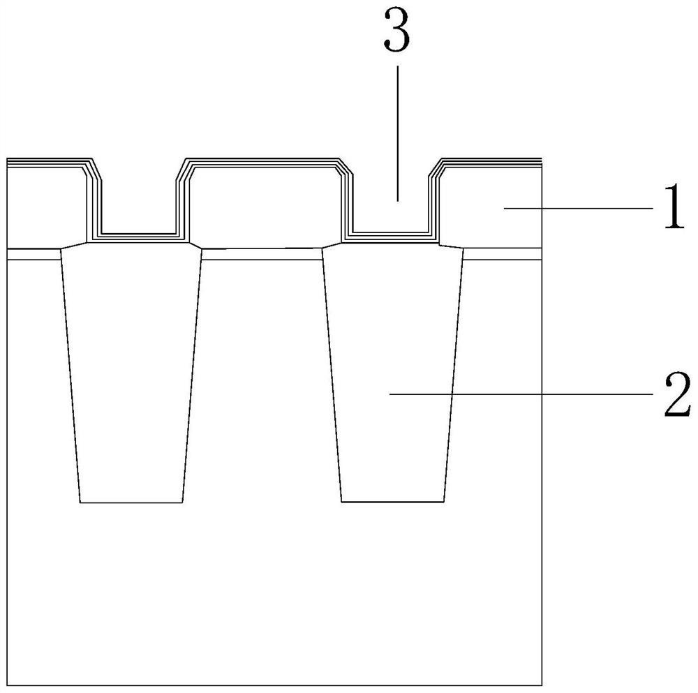
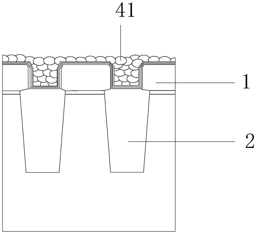
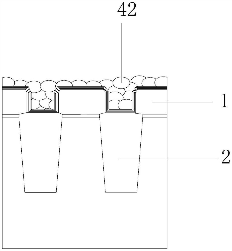
[0038] In a preferred real-time example of the present invention, according to Figure 4 As shown, a method for...


PUM


Abstract

The invention discloses a method for improving control gate filling defects. Polysilicon is deposited at a lower temperature on the surface of a semiconductor structure with a floating gate structure to form a polysilicon layer, and then the silicon wafer is subjected to high-temperature annealing treatment to make the polysilicon secondary grow. By adopting the technical solution of the invention, void defects during filling of polysilicon can be eliminated, while the resistance value of polysilicon and the mobility of carriers are kept unchanged, meeting the process requirements.

Description

technical field [0001] The invention relates to the field of semiconductor manufacturing, in particular to a method for improving control gate filling defects. Background technique [0002] In the existing manufacturing process of semiconductor memory, the process of forming a control gate on the wafer surface is included. In an existing process for forming a control gate, a polysilicon deposition process under high temperature conditions is usually used. However, polysilicon not only has a faster deposition rate but also has a larger grain size under high temperature conditions. Therefore, the polysilicon deposited in the high-aspect-ratio floating gate space in the existing process will form voids, resulting in a decrease in the contact area between the control gate and the floating gate, and ultimately affecting the coupling rate of the device. [0003] As the device size gradually decreases, the opening of the trench between the floating gates becomes smaller and small...

Claims


Application Information

Patent Timeline
Patent Type & Authority Patents(China)
IPC IPC(8): H01L21/28H01L27/11526
CPCH01L29/401H10B41/40
Inventor 黄胜男谢峰周俊
Owner WUHAN XINXIN SEMICON MFG CO LTD
Why Eureka
Try Eureka