Patterned substrate and light emitting diode wafer
A light-emitting diode and patterning technology, applied in electrical components, electrical solid-state devices, circuits, etc., can solve the problems of reducing epitaxial quality and tunneling difference, improving epitaxial quality, reducing compressive stress and tunneling difference. row effect
- Summary
- Abstract
- Description
- Claims
- Application Information
AI Technical Summary
Problems solved by technology
Method used
Image

Examples
Embodiment Construction
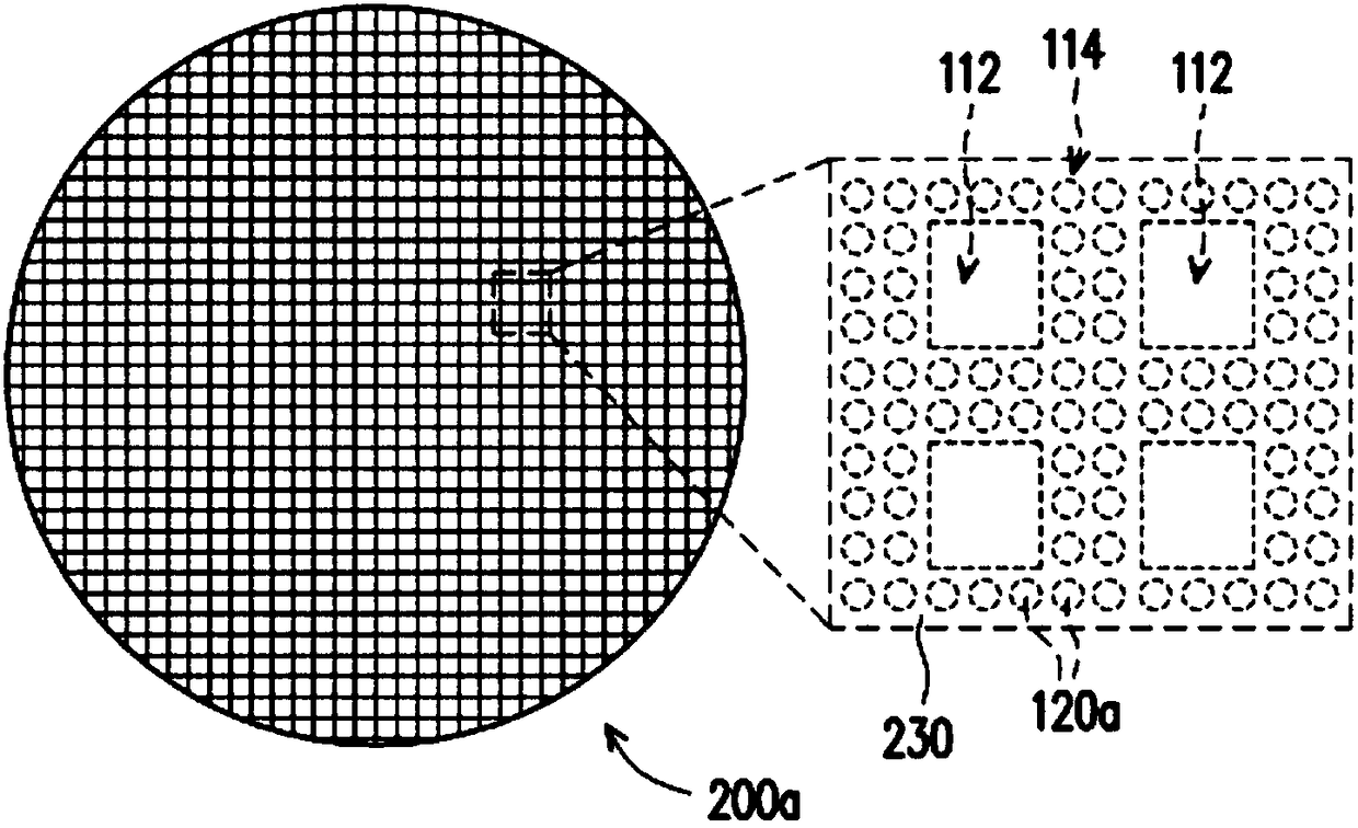
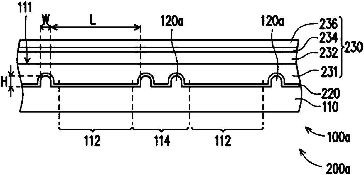
[0050] Figure 1A A schematic top view of an LED wafer according to an embodiment of the present invention is shown. Figure 1B shown as Figure 1A A partial cross-sectional schematic of a light-emitting diode wafer. Please also refer to Figure 1A and Figure 1B , the LED wafer 200a of this embodiment includes a patterned substrate 100a , a buffer layer 220 and an epitaxial structure layer 230 . The patterned substrate 100a of this embodiment includes a substrate 110 and a plurality of pattern structures 120a. The substrate 110 has at least one device configuration area 112 ( Figure 1A and Figure 1B Schematically shows a plurality of) and the cutting area 114 surrounding the component placement area 112 . The pattern structure 120 a is integrally formed with the substrate 110 and located in the cutting area 114 of the substrate 110 . The pattern structures 120 a are separated from each other and distributed in the cutting area 114 .
[0051] In detail, the patterned su...
PUM
| Property | Measurement | Unit |
|---|---|---|
| Width | aaaaa | aaaaa |
Abstract
Description
Claims
Application Information
 - R&D
- Intellectual Property
- Life Sciences
- Materials
- Tech Scout
- Unparalleled Data Quality
- Higher Quality Content
- 60% Fewer Hallucinations
Browse by: Latest US Patents, China's latest patents, Technical Efficacy Thesaurus, Application Domain, Technology Topic, Popular Technical Reports.
© 2025 PatSnap. All rights reserved.Legal|Privacy policy|Modern Slavery Act Transparency Statement|Sitemap|About US| Contact US: help@patsnap.com