2d photonic crystal surface emission laser and method for producing same

一种二维光子晶体、面发光激光器的技术,应用在半导体激光器、激光器、声子激发器等方向,能够解决难以减小光点面积、很难减小光点面积高的光输出、激光波阵面紊乱等问题,达到加大强度、自由度变高、加大面积的效果

Active Publication Date: 2018-10-23
KYOTO UNIV +3
View PDF12 Cites 8 Cited by
  • Summary
  • Abstract
  • Description
  • Claims
  • Application Information

AI Technical Summary

Problems solved by technology

However, in semiconductor lasers, as the emission area is increased, laser oscillation occurs in more modes, so the wavefront of laser light is disturbed
If the wavefront of the laser light is disturbed, it is difficult to reduce the spot area even if the light is condensed by an optical system
Therefore, in the semiconductor lasers currently in practical use, it is difficult to obtain high light output while reducing the spot area.

Method used


Image

  • 2d photonic crystal surface emission laser and method for producing same
  • 2d photonic crystal surface emission laser and method for producing same
  • 2d photonic crystal surface emission laser and method for producing same

Examples


Embodiment Construction

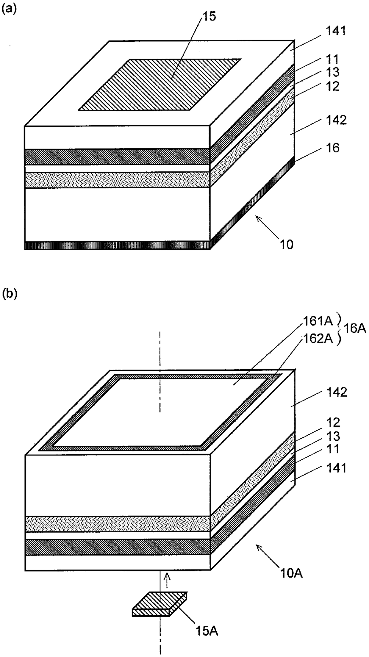
[0060] use Figure 1 to Figure 19 Embodiments of the two-dimensional photonic crystal surface emitting laser according to the present invention will be described.

[0061] (1) Structure of the two-dimensional photonic crystal surface emitting laser of the present embodiment

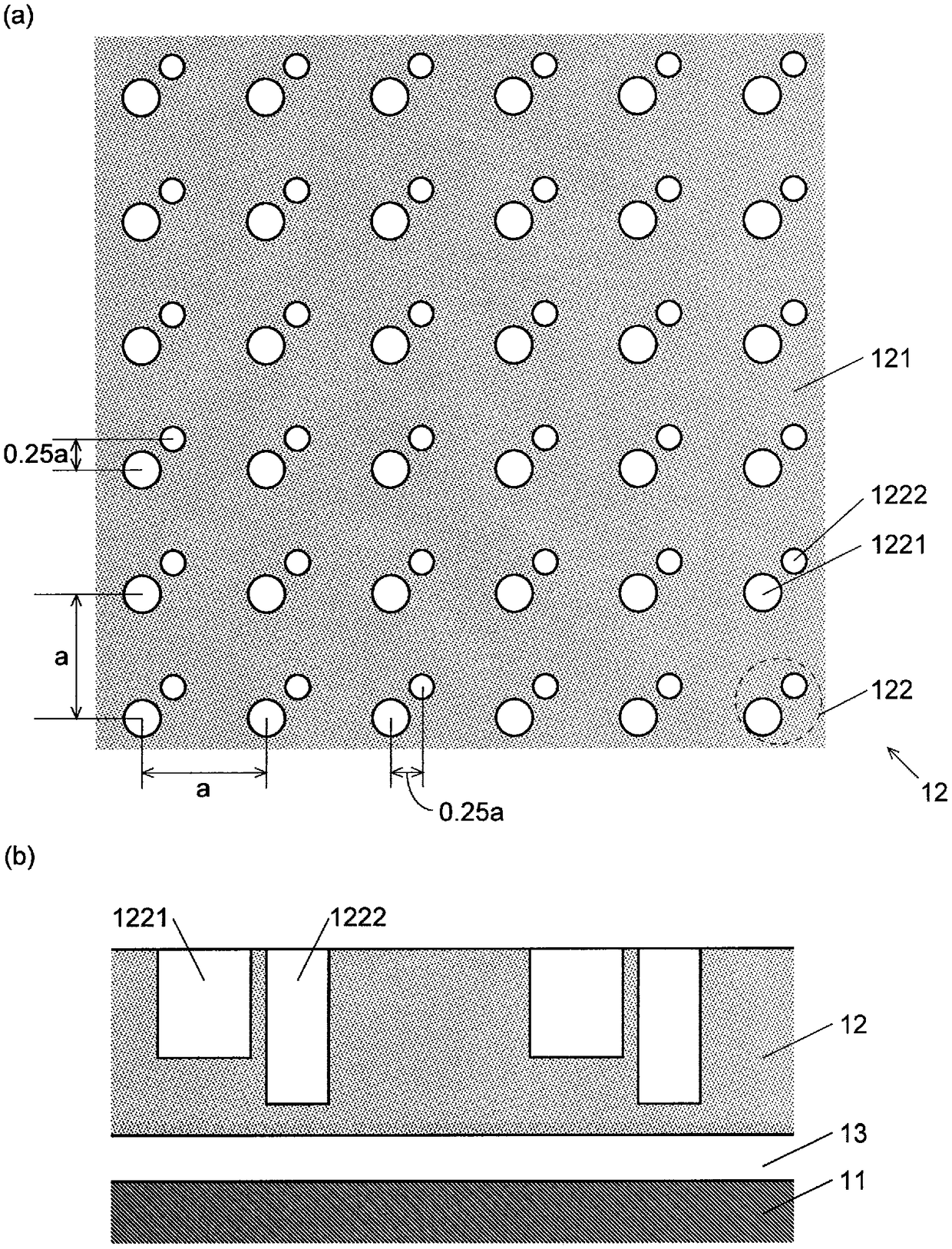
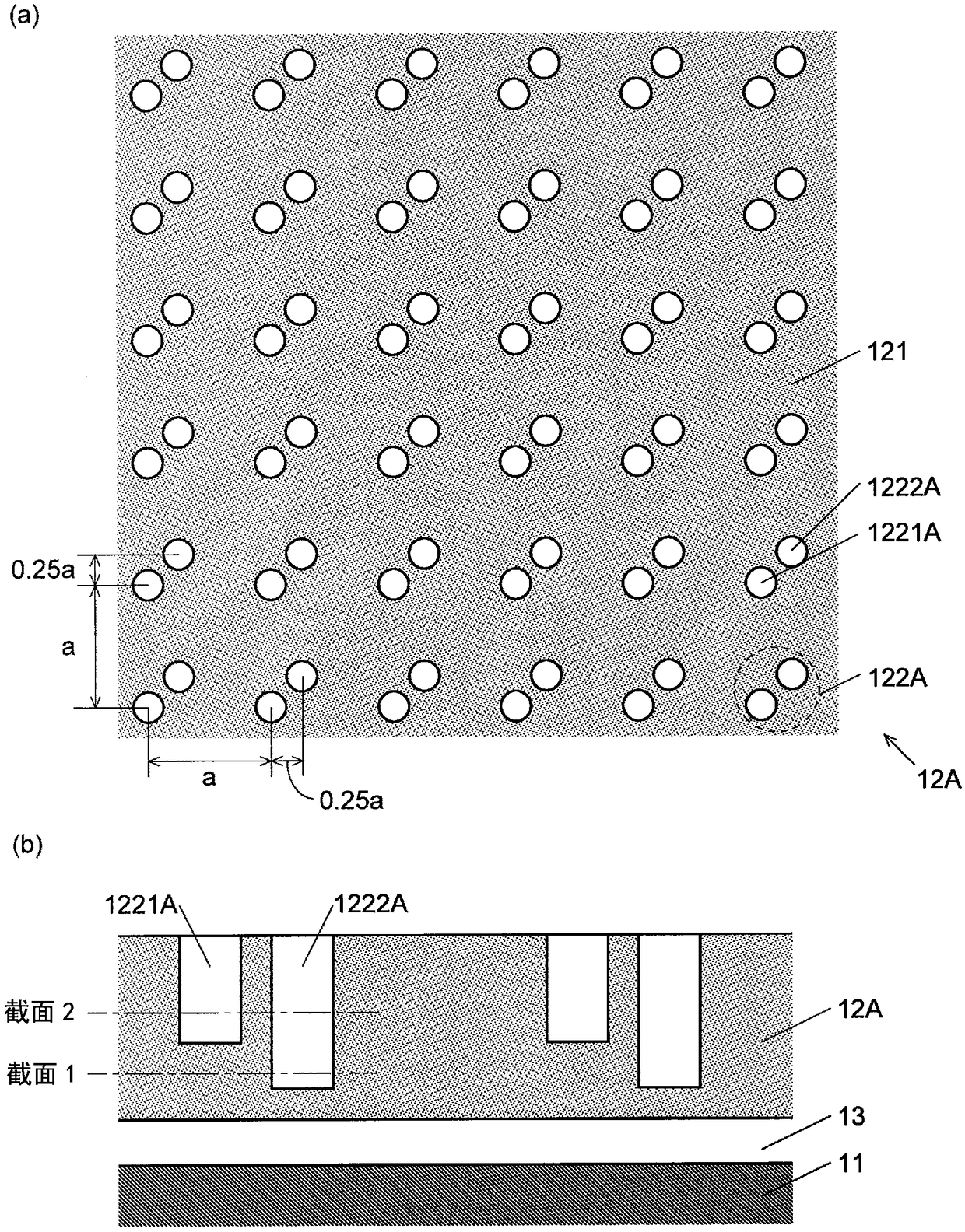
[0062] The two-dimensional photonic crystal surface emitting laser 10 of the present embodiment is as figure 1 As shown in (a), it has the order of the first electrode 15, the first cladding layer 141, the active layer 11, the spacer layer 13, the two-dimensional photonic crystal layer 12, the second cladding layer 142, and the second electrode 16. A structure that stacks them. Wherein, the order of the active layer 11 and the two-dimensional photonic crystal layer 12 can be reversed to the above. exist figure 1 In (a), for convenience, the first electrode 15 is shown as the upper side, and the second electrode 16 is shown as the lower side, but the orientation of the two-dimensional photonic crystal ...


PUM


Abstract

This 2D photonic crystal surface emission laser 10 comprises: a 2D photonic crystal layer 12 having a different refractive index region 122, which comprises a first different refractive index region 1221 and a second different refractive index region 1222 having different refractive indices to a plate-like base material 121, positioned cyclically on the base material 121; and an active layer 11 provided to one side of the base material 121, wherein the planar shape of the first different refractive index region 1211 has a surface area that is greater than or equal to the planar shape of the second different refractive index region 1222, and the first different refractive index region 1221 is thinner than the second different refractive index region 1222. As a result of this configuration,it is possible to have the volumes of the first different refractive index region 1221 and the second different refractive index region 1222 approximate one another, increase the effect of interference of light, the propagation direction of which varies between the two different refractive index regions, and thus obtain laser light having a higher output.

Description

technical field [0001] The invention relates to a semiconductor laser, in particular to a two-dimensional photonic crystal surface-emitting laser for amplifying light by using a two-dimensional photonic crystal and a manufacturing method thereof. Background technique [0002] Semiconductor lasers have many advantages such as small size, low cost, low power consumption, and long life, and are widely used in a wide range of fields such as optical recording light sources, communication light sources, laser displays, laser printers, and laser pointers. On the other hand, in the field of laser processing, a laser having an optical output exceeding at least 1 W is required, but semiconductor lasers currently in practical use cannot achieve this output for the following reasons. Therefore, currently, in the field of laser processing, gas lasers such as carbon dioxide lasers are used instead of semiconductor lasers. [0003] The reason why the optical output of semiconductor lasers...

Claims


Application Information

Patent Timeline
Patent Type & Authority Applications(China)
IPC IPC(8): H01S5/183H01S5/185
CPCH01S5/2027H01S5/04253H01S5/34313H01S5/04254H01S5/04256H01S5/11H01S5/185H01S5/323H01S5/204H01S5/183H01S5/3432H01S2301/17
Inventor 野田进田中良典梅纳卡·德·索伊萨
Owner KYOTO UNIV
Why Eureka
Try Eureka