A semiconductor wafer etching device

An etching device and semiconductor technology, applied in the manufacture of semiconductor/solid-state devices, discharge tubes, electrical components, etc., can solve problems such as damage to the lower electrode plate, achieve the effects of isolating contact, improving etching efficiency, and reducing the number

Active Publication Date: 2020-09-04
无锡中硅新阳科技有限公司
View PDF6 Cites 0 Cited by
  • Summary
  • Abstract
  • Description
  • Claims
  • Application Information

AI Technical Summary

Problems solved by technology

In this technical scheme, the edge protection plate and the ring protection plate are used to slow down the damage of the lower electrode plate, but as the gap between the edge protection plate, the ring protection plate and the electrostatic adsorption platform expands, the plasma will pass through the gap to the lower electrode plate. electrode plate, causing damage to the lower electrode plate

Method used


Image

  • A semiconductor wafer etching device
  • A semiconductor wafer etching device
  • A semiconductor wafer etching device

Examples


Embodiment Construction

[0023] In order to make the technical means, creative features, goals and effects achieved by the present invention easy to understand, the present invention will be further described below in conjunction with specific embodiments.

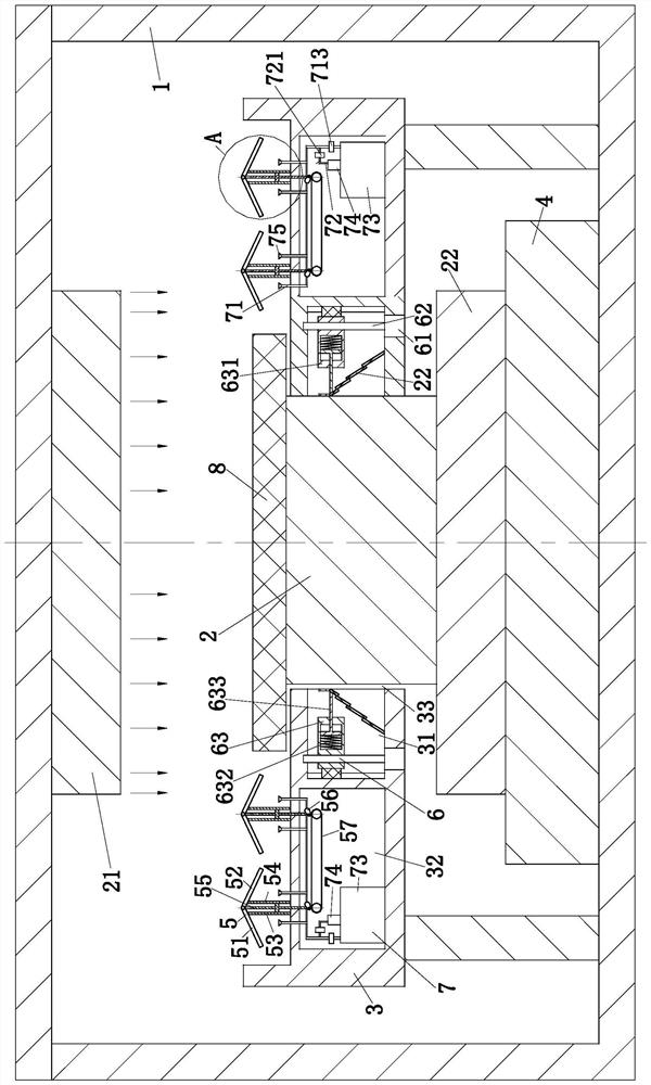
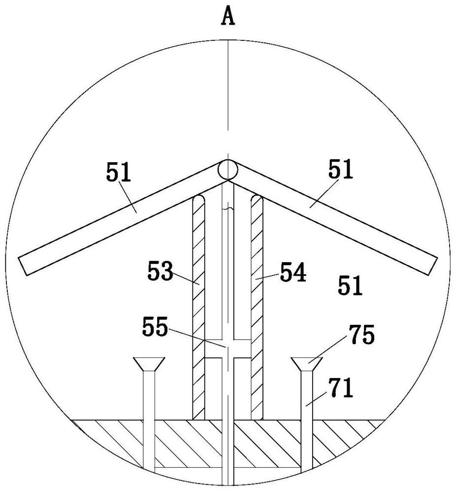
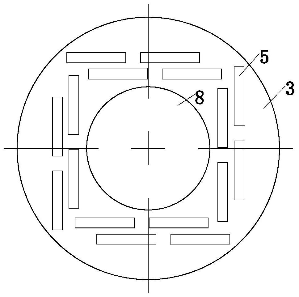
[0024] Such as Figure 1-5 As shown, a semiconductor wafer etching device includes an airtight casing 1, an electrostatic adsorption platform 2, an upper electrode plate 21, a lower electrode plate 22, an annular insulating protection plate 3, an insulating base 4, an ion buffer module 5, and an automatic gap The compensation module 6 and the ion extraction module 7, the inside of the airtight casing 1 is a vacuum environment; the upper electrode plate 21 is located in the center of the top of the airtight casing 1; the insulating base 4 is located at the bottom of the airtight casing 1, The insulating base 4 is used to support the electrostatic adsorption platform 2; the electrostatic adsorption platform 2 is located at the upper end of the insul...


PUM

PropertyMeasurementUnit
thicknessaaaaaaaaaa

Abstract

The invention belongs to the technical field of semiconductor wafer manufacturing and particularly discloses a semiconductor wafer etching system. The semiconductor wafer etching system comprises a closed shell, an electrostatic adsorption platform, an upper electrode plate, a lower electrode plate, an annular insulating protection plate, an insulating base, an ion buffer module, an automatic clearance compensation module and an ion extraction module. According to the semiconductor wafer etching system, the condition that arc discharge is generated to know down the lower electrode plate afterplasma A and the lower electrode plate are conducted can be effectively reduced or avoided through coordinated working of the ion buffer module, the automatic clearance compensation module and the ionextraction module, and the service life of the semiconductor wafer etching system is prolonged.

Description

technical field [0001] The invention belongs to the technical field of semiconductor wafer manufacturing, in particular to a semiconductor wafer etching device. Background technique [0002] Wafer refers to the silicon wafer used in the production of silicon semiconductor integrated circuits. Because of its circular shape, it is called a wafer. It can be processed into various circuit element structures on the silicon wafer and become an IC with specific electrical functions. product. [0003] Around the wafer, there are platforms for placing the wafer, insulators supporting the wafer, insulators supporting the lower electrode plate, and other structures. When the plasma touches the insulating object, the electrons in the plasma are light in weight, fast in movement, The activity is violent, a large number of light, active, and negatively charged electrons are attached to the insulating object, making the insulating object negatively charged. When the negative potential on ...

Claims


Application Information

Patent Timeline
Patent Type & Authority Patents(China)
IPC IPC(8): H01L21/67H01J37/32
CPCH01J37/32623H01J37/32807H01L21/67069
Inventor 侯玉闯薛鹏
Owner 无锡中硅新阳科技有限公司
Why Eureka
Try Eureka