
Wide base region lumped electric charge modeling method for large-power bipolar semiconductor device

A modeling method and semiconductor technology, applied in the fields of instruments, electrical digital data processing, special data processing applications, etc., can solve the problems of mixed model parameters, low simulation accuracy, high numerical model accuracy, and achieve clear definition and representation. Improve simulation accuracy and reduce complexity

Active Publication Date: 2018-11-06
NAVAL UNIV OF ENG PLA
View PDF3 Cites 5 Cited by
  • Summary
  • Abstract
  • Description
  • Claims
  • Application Information

AI Technical Summary

Problems solved by technology

The behavioral model is weak in guiding the design and application of the device because it cannot describe the internal characteristics of the device; the numerical model has high precision but the calculation load is large, and some structural parameters need to be provided by the manufacturer; the parameters of the mixed model are mixed and the versatility is not high
The physical parameters in the physical model are not clear, the values ​​are extracted by fitting, and the simulation accuracy is low

Method used


Image

  • Wide base region lumped electric charge modeling method for large-power bipolar semiconductor device
  • Wide base region lumped electric charge modeling method for large-power bipolar semiconductor device
  • Wide base region lumped electric charge modeling method for large-power bipolar semiconductor device

Examples


Embodiment Construction

[0027] The present invention will be further described in detail below in conjunction with the accompanying drawings and specific embodiments to facilitate a clear understanding of the present invention, but they do not limit the present invention.

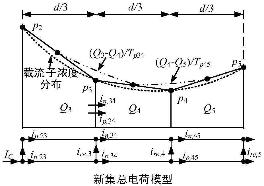
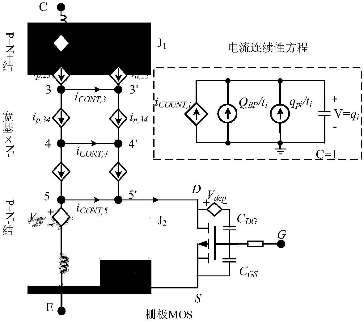
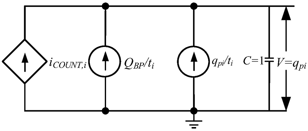
[0028] Such as figure 1 As shown, the present invention divides the wide base area into n areas with equal width, and uses n lumped charges to represent the charge distribution in the n areas respectively, n≥3, that is, n is an integer greater than or equal to 3, according to the area The charge distribution and charge motion mechanism define drift current and diffusion current, determine the hole current and electron current between adjacent regions through the current density equation, and determine the recombination current caused by the charge in each region according to the current continuity equation, and use the hole current , electron current and recombination current as the basis to establish a lumped charge model with a ...


PUM


Abstract

The invention discloses a wide base region lumped electric charge modeling method for a large-power bipolar semiconductor device. A wide base region is divided into n areas with equal width, and n pieces of lumped electric charges are adopted for independently expressing electric charge distribution in the n pieces of areas, wherein n is greater than or equal to 3; according to the electric chargedistribution of the area and an electric charge motion mechanism, drift current and diffusion current are defined; through a current density equation, hole current and electron current between adjacent areas are determined; according to a current continuity equation, recombination current caused by electric charges in each area is determined; and the hole current, the electron current and the recombination current are taken as a basis to establish a wide base region lumped electric charge model. By use of the method, the simulation accuracy of the wide base region lumped electric charge modelis improved, and therefore, the accurate calculation of an electric charge quantity in the wide base region of the large-power bipolar semiconductor device under multiple working conditions is realized.

Description

technical field [0001] The invention belongs to the technical field of power electronic device modeling and its application, and in particular relates to a method for modeling lumped charge in a wide base region of a high-power bipolar semiconductor device. Background technique [0002] At present and in the foreseeable future, a large number of power electronic switching devices will be used in fields requiring energy conversion such as new energy, motor drive, aerospace, high-speed rail, ship propulsion, and power transmission. Bipolar semiconductor power electronic devices such as IGBT (Insulated Gate Bipolar Transistor, Insulated Gate Bipolar Transistor) have the advantages of large power level, easy driving and protection, high switching frequency, and excellent comprehensive performance. Investigations show that the market application of IGBT power levels in power electronic devices above 10kV and 300A occupies an absolute majority. [0003] The design and manufacture...

Claims


Application Information

Patent Timeline
IPC IPC(8): G06F17/50
CPCG06F30/367
Inventor 段耀强李鑫罗毅飞刘宾礼黄永乐肖飞
Owner NAVAL UNIV OF ENG PLA
Learn More