OLED screen used as light source for fingerprint identification device and optical fingerprint identification device

A technology of fingerprint identification and light source, which is applied in the direction of acquiring/arranging fingerprints/palmprints, character and pattern recognition, and electric solid-state devices. It can solve the problems of large signal noise and poor imaging quality, and achieve the goal of improving device performance and shielding interference. Effect

Active Publication Date: 2022-03-18
GUAN YEOLIGHT TECH CO LTD
View PDF6 Cites 0 Cited by
  • Summary
  • Abstract
  • Description
  • Claims
  • Application Information

AI Technical Summary

Problems solved by technology

[0005] Therefore, the technical problem to be solved by the present invention is to overcome the defects of relatively large signal noise and poor imaging quality when OLED is used as a light source of a fingerprint identification device in the prior art, thereby providing an optical fingerprint identification device, the light source of which adopts The improved OLED transparent screen, due to the use of an opaque first electrode layer with a microporous structure, can effectively reduce the interference of the light emitted by the OLED screen itself on the detector, thus making the image clearer

Method used


Image

  • OLED screen used as light source for fingerprint identification device and optical fingerprint identification device
  • OLED screen used as light source for fingerprint identification device and optical fingerprint identification device
  • OLED screen used as light source for fingerprint identification device and optical fingerprint identification device

Examples


Embodiment 1

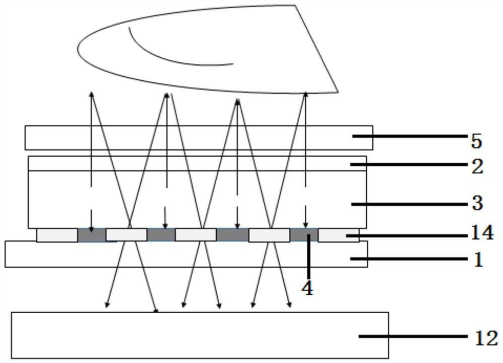
[0038] like figure 1As shown, the optical fingerprint identification device in this embodiment includes an OLED screen body and an optical sensor 12, the optical sensor 12 is arranged on a side away from the light-emitting surface of the OLED screen body, and the light source OLED screen body is an upright OLED screen bodies, including:

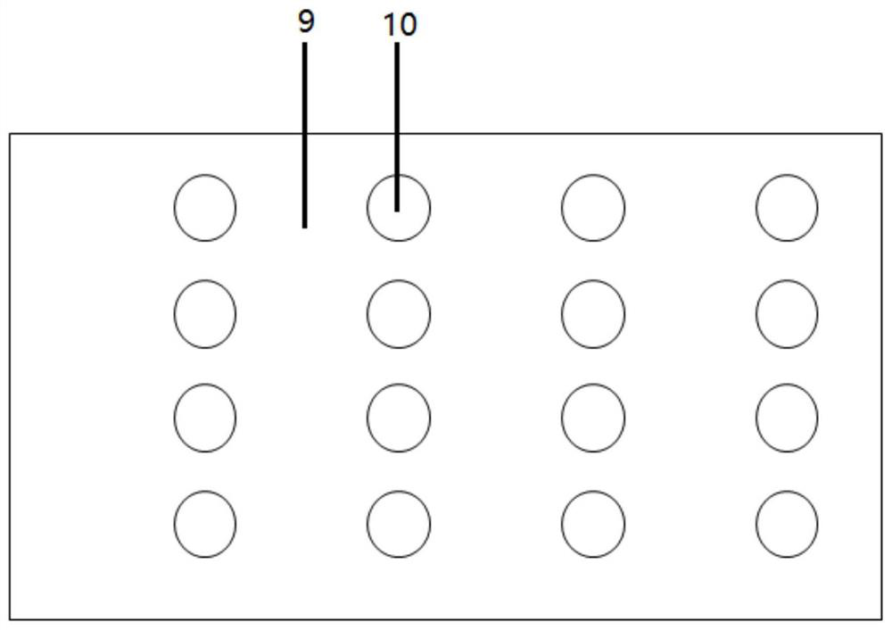
[0039] A transparent substrate 1 and an encapsulation cover 5, the transparent substrate 1 is provided with an opaque first electrode layer 4, an organic light-emitting unit 3 and a transparent second electrode layer 2, and the opaque first electrode layer 4 is provided with a number of micropores 10. The micropore 10 is filled with a transparent insulating layer 14, and the opaque first electrode layer 4 is a metal layer with a work function greater than 5eV, used as an opaque anode, preferably, the opaque anode is an Au or Pt metal layer , with a thickness of 10nm to 10um.

[0040] The transparent insulating layer 14 can adopt figure 1 T...

Embodiment 2

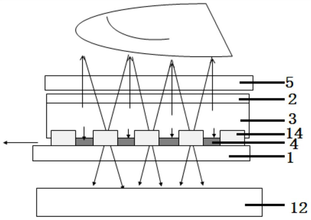
[0052] Such as figure 1 as shown in figure 1 As shown, the optical fingerprint identification device in this embodiment includes an OLED screen body and an optical sensor 12, the optical sensor 12 is arranged on a side away from the light-emitting surface of the OLED screen body, and the light source OLED screen body is a positive OLED screen bodies, including:

[0053] A transparent substrate 1 and an encapsulation cover 5, the transparent substrate 1 is provided with an opaque first electrode layer 4, an organic light-emitting unit 3 and a transparent second electrode layer 2, and the opaque first electrode layer 4 is provided with a number of micropores 10. The micropore 10 is filled with a transparent insulating layer 14, and the opaque first electrode layer 4 is a metal layer with a work function of less than 4.5 eV, which is used as an opaque reflective cathode, and the OLED device adopts an inverted structure. Preferably, The opaque reflective cathode is a metal layer...


PUM

PropertyMeasurementUnit
electron work functionaaaaaaaaaa
thicknessaaaaaaaaaa
electron work functionaaaaaaaaaa

Abstract

The invention provides an OLED screen used as a light source for a fingerprint identification device and an optical fingerprint identification device, the optical fingerprint identification device includes an OLED screen and an optical sensor, and the optical sensor is arranged on a light-emitting surface far away from the OLED screen On one side of the OLED screen, an opaque first electrode layer, an organic light-emitting unit, and a transparent or semi-transparent second electrode layer are arranged on the transparent substrate of the OLED screen, and a number of micropores are arranged on the opaque first electrode layer, so that The microholes are filled with a transparent insulating layer and / or covered by a transparent insulating layer; when a finger touches and presses the light-emitting surface of the OLED screen body, after the light emitted by the light-emitting area is reflected by the finger, part of the light passes through the After the microhole reaches the optical sensor to form a fingerprint identification signal. The OLED transparent screen of the present invention uses the electrode layer with a microporous structure directly as the opaque microporous layer, which saves the process, and at the same time, the present invention can effectively reduce the interference of the light emitted by the OLED screen itself on the detector , making the image clearer.

Description

technical field [0001] The invention relates to the technical field of optical fingerprint identification devices, in particular to an optical fingerprint identification device using an OLED display screen as a light source. Background technique [0002] The optical fingerprint collector is an optical fingerprint collector that requires its own light source. The current light source uses LED chips and light guide plates, which have the disadvantages of low energy efficiency, uneven illumination, high assembly requirements, and high cost. [0003] Since the organic electroluminescent device (English full name is Organic Light Emitting Device, referred to as OLED) has the advantages of fast response, no pollution, high contrast, planarization, and thinness, people try to use OLED to replace the light source in the optical fingerprint collector. The invention overcomes the deficiency when the LED chip and the light guide plate are used as the light source in the optical fingerp...

Claims


Application Information

Patent Timeline
Patent Type & Authority Patents(China)
IPC IPC(8): G06V40/13H01L51/52
CPCG06V40/1318H10K50/813H10K50/822
Inventor 李曼朱映光郭立雪胡永岚
Owner GUAN YEOLIGHT TECH CO LTD
Why Eureka
Try Eureka