Fin field-effect transistor and forming method thereof

A fin-type field effect transistor and a layer-forming technology are applied in transistors, semiconductor devices, electrical components, etc., and can solve the problems that the electrical performance of the fin-type field effect transistor needs to be improved.

Inactive Publication Date: 2018-11-13
SEMICON MFG INT (SHANGHAI) CORP +1
View PDF9 Cites 2 Cited by
  • Summary
  • Abstract
  • Description
  • Claims
  • Application Information

AI Technical Summary

Problems solved by technology

[0006] The electrical performance of the fin field effect transistor formed by the prior art needs to be improved

Method used


Image

  • Fin field-effect transistor and forming method thereof
  • Fin field-effect transistor and forming method thereof
  • Fin field-effect transistor and forming method thereof

Examples


Embodiment Construction

[0024] The electrical performance of the fin field effect transistor formed according to the background technology needs to be improved. The reason why the electrical performance of the FinFET needs to be improved is analyzed in conjunction with the formation process of the FinFET.

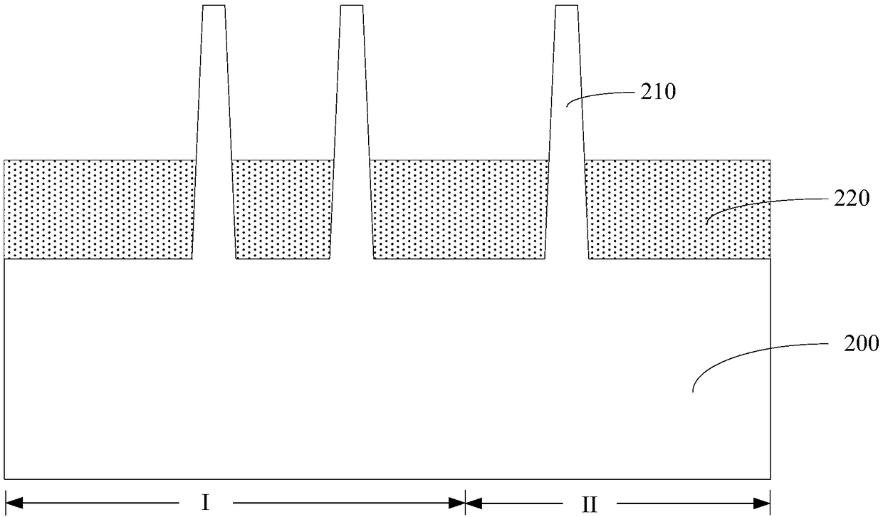
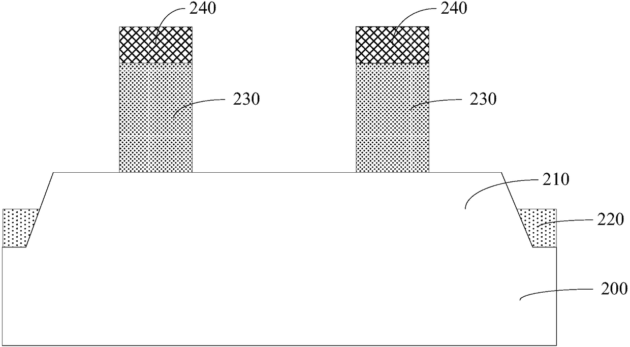
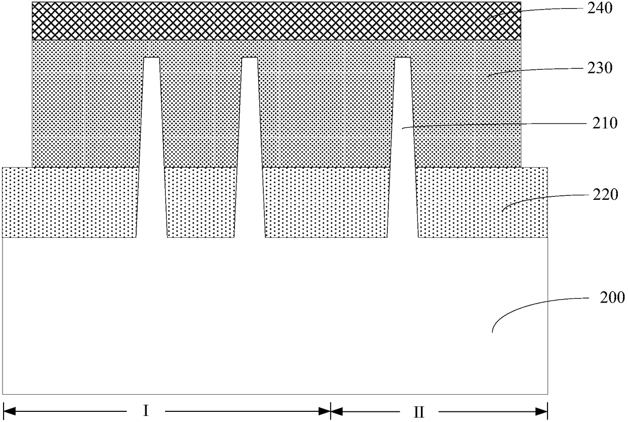
[0025] The forming method includes: providing a substrate, the substrate including a first device region and a second device region, and having a plurality of discrete fins on the substrate; forming a dummy gate across the fins ; forming an interlayer dielectric layer on the exposed fin of the dummy gate, the interlayer dielectric layer exposing the dummy gate; performing patterning on the dummy gate, in the interlayer dielectric layer forming a first opening, and in a direction perpendicular to the surface of the substrate, the first opening penetrates the dummy gate; forming a dielectric layer filling the first opening; removing the dummy gate in the forming a second opening and a third opening...


PUM


Abstract

The invention provides a fin field-effect transistor and a forming method thereof. The forming method comprises: providing a substrate, the substrate including a first device region and a second device region, and the substrate having a plurality of discrete fins; forming a dummy grid electrode across the fins; forming an interlayer dielectric layer on the fins exposed the dummy grid electrode, the interlayer dielectric layer exposing the dummy grid electrode; removing a first opening of the dummy grid electrode, the first opening formed in the interlayer dielectric layer; forming an initial metal grid electrode fully filling the first opening; performing graphical processing on the initial metal grid electrode, to form a second opening in the initial metal grid electrode, on the directionvertical to a substrate surface, the second opening penetrating the initial metal grid electrode; forming a first metal grid electrode in the first device region and forming a second metal grid electrode in the second device region. Electrical properties of the fin field-effect transistor are improved.

Description

technical field [0001] The invention relates to the technical field of semiconductor manufacturing, in particular to a fin field effect transistor and a forming method thereof. Background technique [0002] With the rapid development of semiconductor technology, the feature size of semiconductor devices is constantly shrinking, which makes the integration of integrated circuits higher and higher, which also puts forward higher requirements for the performance of devices. [0003] Currently, as the size of Metal-Oxide Semiconductor Field Effect Transistors (MOSFETs) continues to decrease. In order to adapt to the reduction of process nodes, the channel length of MOSFET field effect transistors can only be continuously shortened. The shortening of the channel length has the advantages of increasing the die density of the chip and increasing the switching speed of the MOSFET field effect tube. [0004] However, as the channel length of the device is shortened, the distance be...

Claims


Application Information

Patent Timeline
Patent Type & Authority Applications(China)
IPC IPC(8): H01L27/088H01L21/8234
CPCH01L21/823431H01L21/823437H01L27/0886H01L21/76224H01L29/66545H01L21/845H01L29/6681H01L29/785H01L21/762H01L29/41791
Inventor 周飞
Owner SEMICON MFG INT (SHANGHAI) CORP
Why Eureka
Try Eureka