A homogeneous pn junction based on two-dimensional semiconductor material and its preparation method

A two-dimensional semiconductor, semiconductor technology, applied in the field of nanoelectronics

Active Publication Date: 2020-07-28
PEKING UNIV
View PDF5 Cites 0 Cited by
  • Summary
  • Abstract
  • Description
  • Claims
  • Application Information

AI Technical Summary

Problems solved by technology

However, it is currently difficult to dope two-dimensional semiconductor materials by ion implantation in experiments to realize PN junctions. In addition, there are stability problems in doping by physical and chemical adsorption, and there are still great challenges in experimental preparation.

Method used


Image

  • A homogeneous pn junction based on two-dimensional semiconductor material and its preparation method
  • A homogeneous pn junction based on two-dimensional semiconductor material and its preparation method
  • A homogeneous pn junction based on two-dimensional semiconductor material and its preparation method

Examples


Embodiment Construction

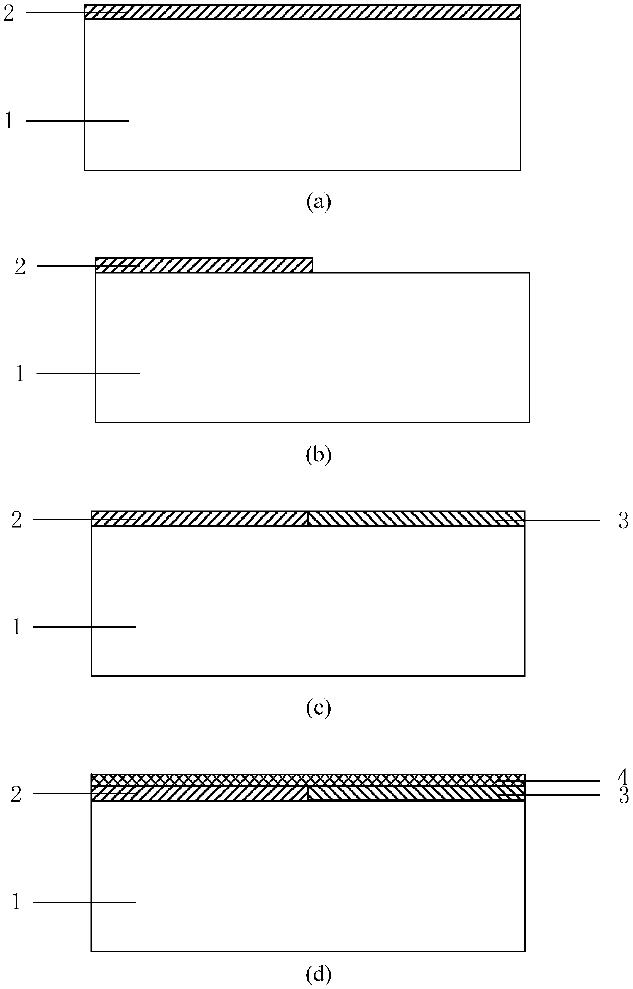
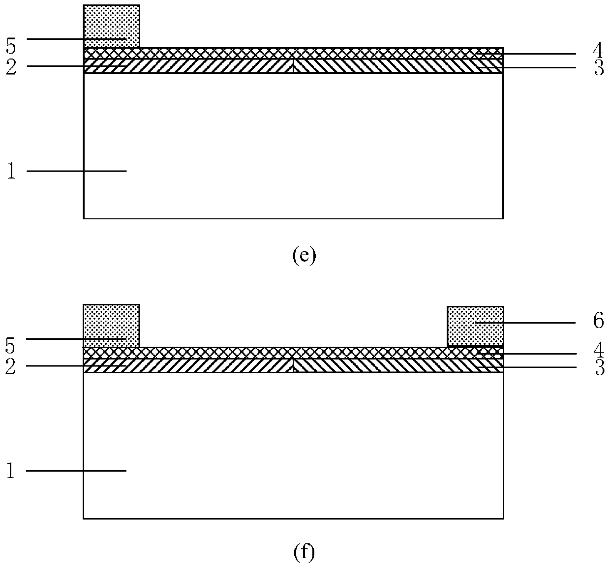
[0036] The present invention will be further described through the embodiments below in conjunction with the accompanying drawings.

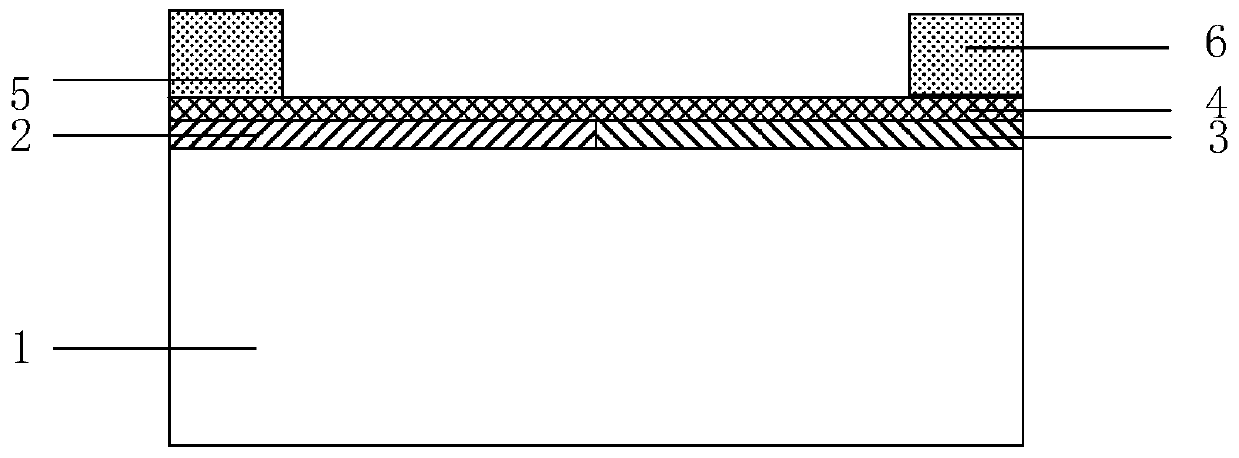
[0037] Such as figure 1As shown, the prepared homogeneous PN junction based on two-dimensional semiconductor materials includes an insulating substrate 1, a first two-dimensional semiconductor material 2, a second two-dimensional semiconductor material 3, a third two-dimensional semiconductor material 4, and a P-type region metal Contact electrode 5 and N-type regional metal contact electrode 6 . Wherein, the first two-dimensional semiconductor material 2 and the second two-dimensional semiconductor material 3 are located on the insulating substrate 1, the third two-dimensional semiconductor material 4 is located above the first two-dimensional semiconductor material 2 and the second two-dimensional semiconductor material 3, P The type region metal contact electrode 5 and the N type region metal contact electrode 6 are respectively located on t...


PUM

PropertyMeasurementUnit
thicknessaaaaaaaaaa
electron work functionaaaaaaaaaa

Abstract

The invention discloses a homogenous PN (positive-negative) junction on the basis of two-dimensional semiconductor materials and a method for preparing the homogenous PN junction. By the aid of the homogenous PN junction and the method, the problems of N-type doping on semiconductor materials with low Fermi energy levels and P-type doping on semiconductor materials with high Fermi energy levels due to the fact that electrons can be transferred to the materials with the low Fermi energy levels from the existing two-dimensional semiconductor materials with the high Fermi energy levels when the two types of semiconductor materials with different work functions are perpendicularly stacked can be solved. The homogenous PN junction and the method have the advantages that the homogenous abrupt PNjunction can be formed in the two-dimensional semiconductor materials by the aid of the doping method, band tails can be prevented from being led into forbidden bands, and the homogenous PN junctionand the method have important significance in electronic device application; the doping method is free of crystal lattice damage due to ion collision, the stability can be greatly enhanced, processesfor preparing the homogenous PN junction are simple, and the homogenous PN junction and the method are easy to popularize to large-scale production.

Description

technical field [0001] The invention belongs to the technical field of nanoelectronics, and in particular relates to a homogeneous PN junction based on a two-dimensional semiconductor material and a preparation method thereof. Background technique [0002] With the reduction of traditional MOSFET feature size and the improvement of integration, the operating voltage and threshold voltage of the device are gradually reduced. The ensuing short-channel effect is more obvious, and the drain-induced barrier reduction and source-drain band-band tunneling will increase the leakage current and power consumption of the device. Due to its atomic-level physical thickness, two-dimensional semiconductor materials can obtain ideal gate control capabilities, and at the same time, large bandgap widths can obtain small leakage currents, which has attracted extensive research and has become a very promising future in the post-silicon era. A class of semiconductor materials. For semiconducto...

Claims


Application Information

Patent Timeline
Patent Type & Authority Patents(China)
IPC IPC(8): H01L29/861H01L21/34
CPCH01L29/66969H01L29/8611H01L29/8613
Inventor 黄如贾润东黄芊芊王慧敏陈亮陈诚赵阳
Owner PEKING UNIV
Why Eureka
Try Eureka