

A silicon-based electroabsorption modulator and its preparation method
An electro-absorption modulator, silicon-based technology, applied in the field of optical interconnection, can solve the problems of complex manufacturing process, complex process, small process tolerance, etc. Effect
- Summary
- Abstract
- Description
- Claims
- Application Information
AI Technical Summary
Problems solved by technology
Method used
Image

Examples
Embodiment Construction
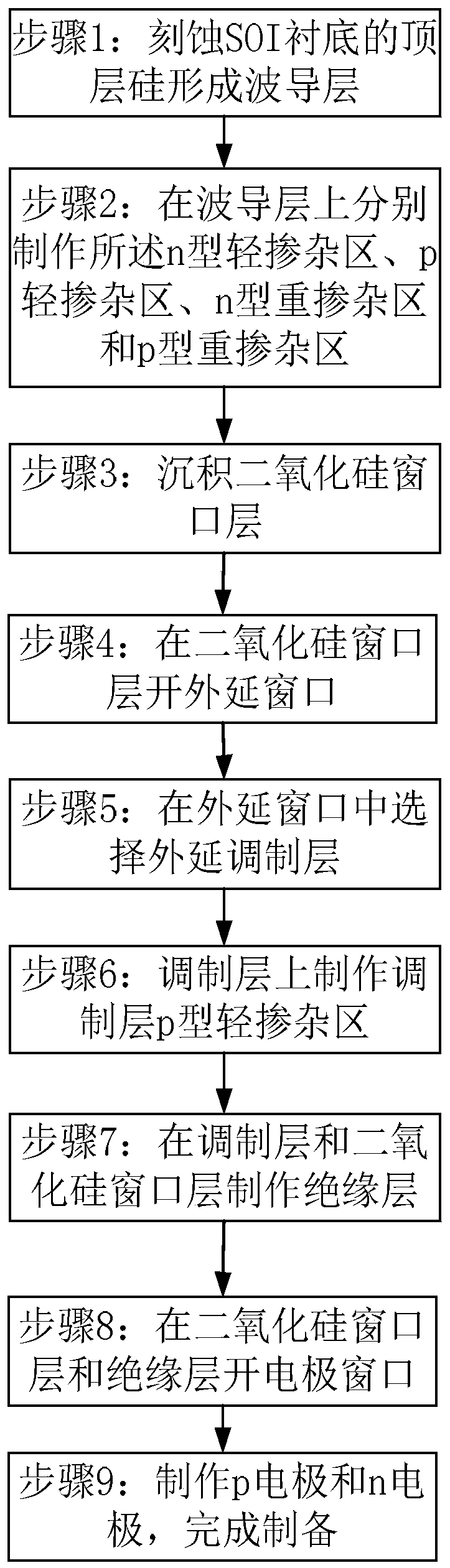
[0039] In order to make the object, technical solution and advantages of the present invention clearer, the present invention will be described in further detail below in conjunction with specific embodiments and with reference to the accompanying drawings.
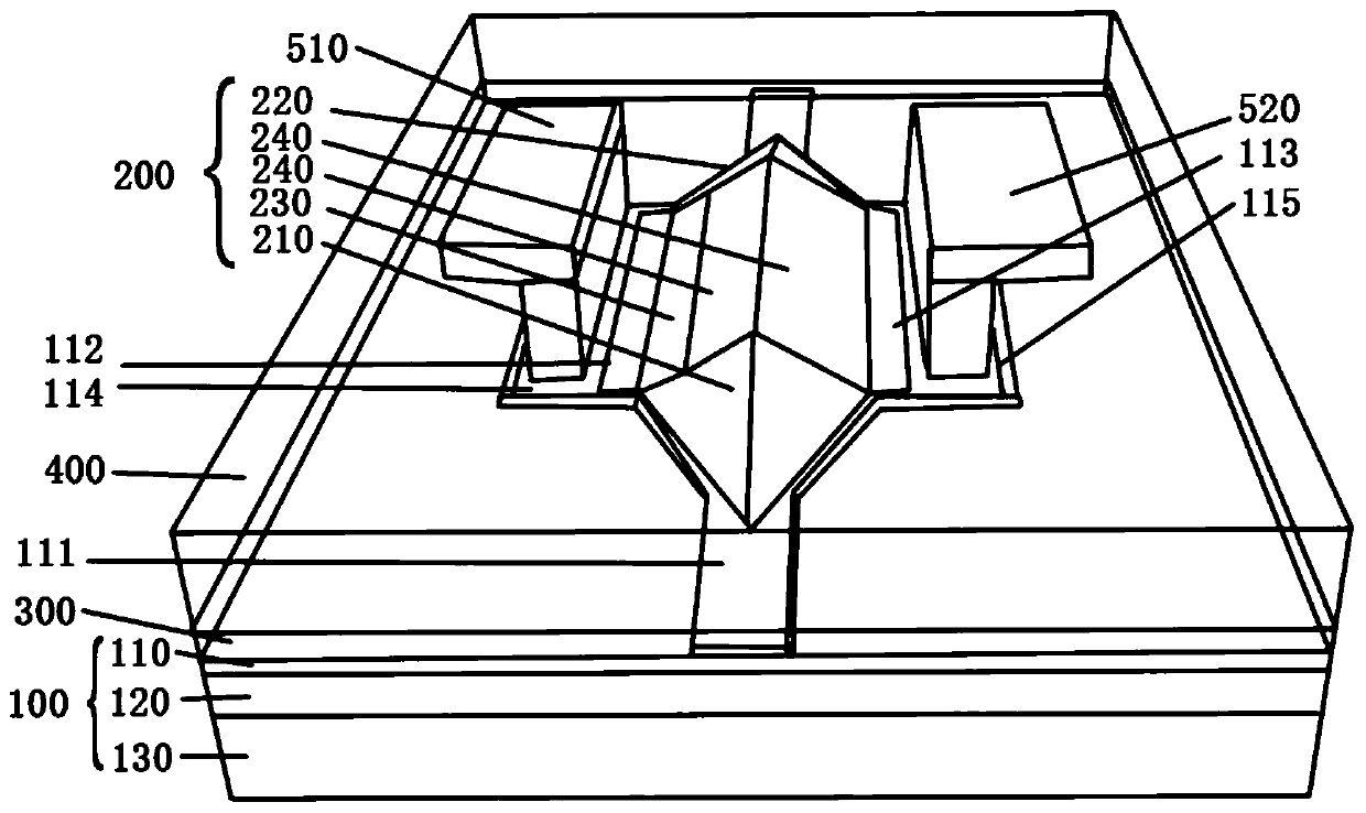
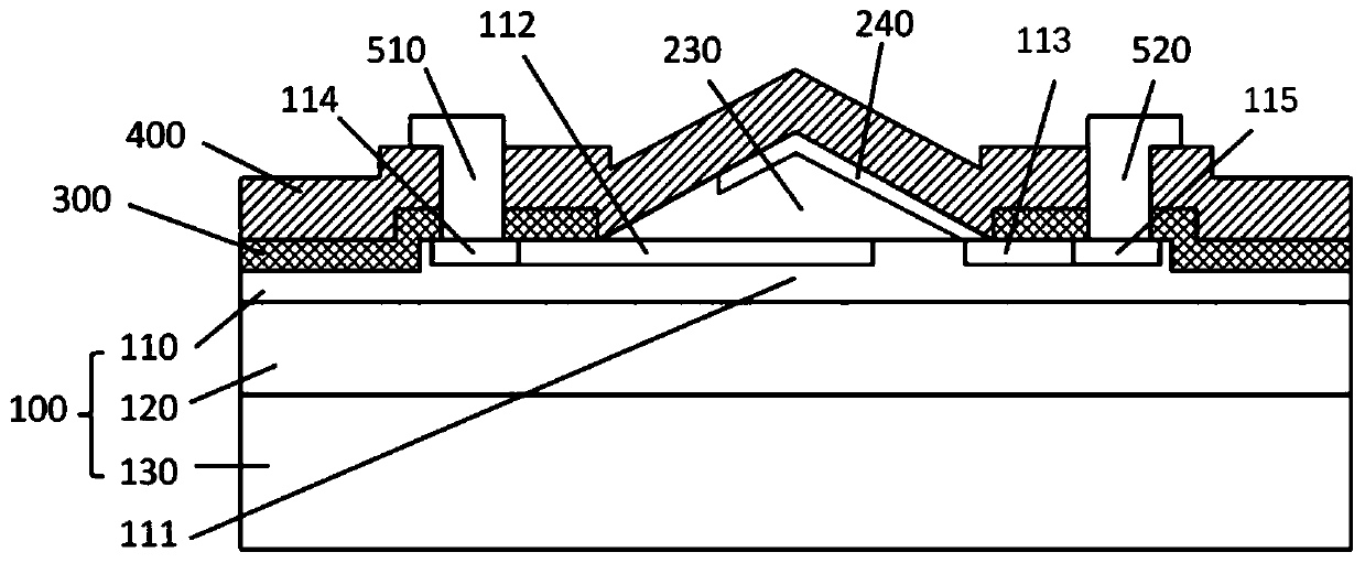
[0040] figure 1 , figure 2 Shown are the three-dimensional structure schematic diagram and the cross-sectional schematic diagram of the silicon-based electro-absorption modulator of the present invention, it can be seen that the silicon-based electro-absorption modulator includes the following parts: SOI substrate 100, doped layer, silicon dioxide window layer 300 , modulation layer 200, insulating medium layer 400 and electrodes.
[0041]SOI substrate 100: the substrate is composed of three parts, from bottom to top are the bottom Si material layer 130, the silicon dioxide buried layer 120 and the top layer of silicon 110, and then engraved on the top layer of silicon 110 of the substrate 100 There is a waveguide laye...
PUM
| Property | Measurement | Unit |
|---|---|---|
| electrical resistivity | aaaaa | aaaaa |
| length | aaaaa | aaaaa |
| thickness | aaaaa | aaaaa |
Abstract
Description
Claims
Application Information