Devices including nanowires and methods of making the same
A production method and nanowire technology, which is applied in semiconductor/solid-state device manufacturing, nanotechnology, semiconductor devices, etc., can solve problems such as the inability to make nanowires, and achieve perfect crystal lattice, high density, and good performance
- Summary
- Abstract
- Description
- Claims
- Application Information
AI Technical Summary
Problems solved by technology
Method used
Image
Examples
Embodiment
[0056] Methods of fabricating devices including nanowires include:
[0057] Provide a silicon substrate;
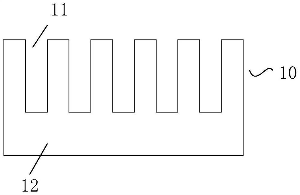
[0058] Using photolithography and plasma etching to dig a plurality of grooves with a width of 20nm (the distance between two adjacent grooves is 40nm) and a depth of 100nm on the silicon substrate, such as figure 1 shown;
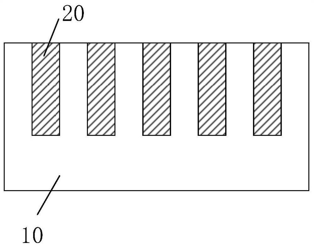
[0059] Using a thermal oxidation process, the substrate is thermally oxidized to form 1nm SiO 2 layer, and then use PECVD to deposit SiO in the groove 2 , and finally perform a CMP planarization process to form a similar figure 2 the structure shown;
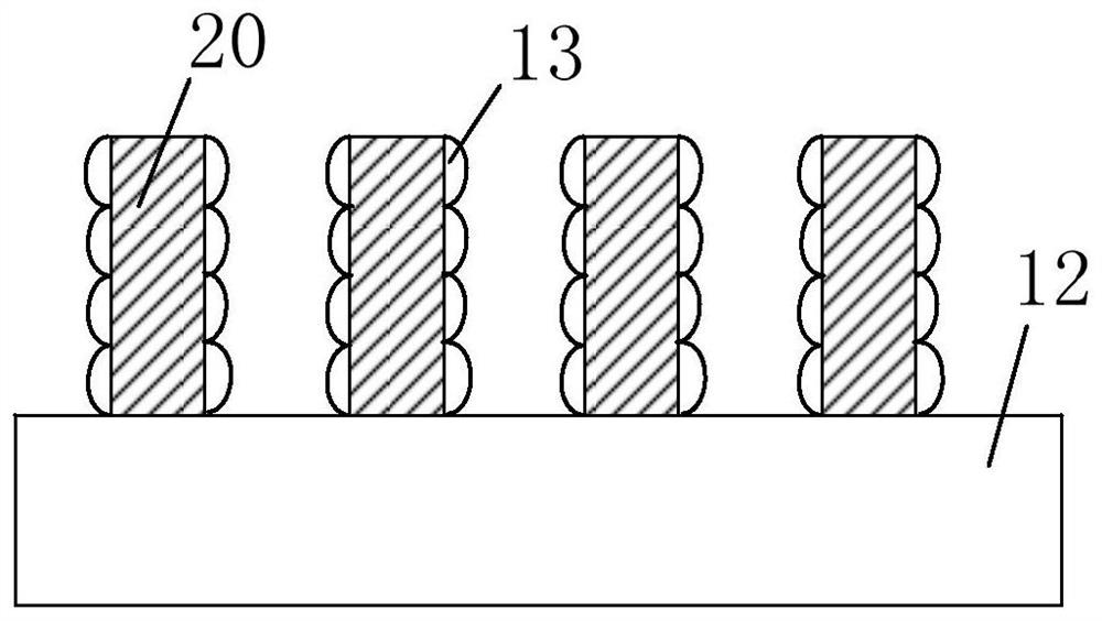
[0060] The second pre-nanowire is obtained by plasma alternate etching of anisotropic etching and isotropic etching, and the etching gas of anisotropic etching is SF 6 +O 2 , the etching gas for isotropic etching is SF 6 , the height of the second pre-nanowire is 3-6 nm;
[0061] Repeat the above process to obtain multiple stacked second pre-nanowires. For details, please refer to image 3 a ...
PUM
| Property | Measurement | Unit |
|---|---|---|
| thickness | aaaaa | aaaaa |
Abstract
Description
Claims
Application Information


