Device comprising nanowires and production method of device

A fabrication method and nanowire technology, applied in semiconductor/solid-state device manufacturing, nanotechnology, semiconductor devices, etc., can solve problems such as inability to fabricate nanowires, and achieve the effect of perfect lattice, good performance, and high density

Active Publication Date: 2018-11-23
INST OF MICROELECTRONICS CHINESE ACAD OF SCI
View PDF3 Cites 0 Cited by
  • Summary
  • Abstract
  • Description
  • Claims
  • Application Information

AI Technical Summary

Problems solved by technology

[0006] The main purpose of the present application is to provide a device including nanowires and its manufacturing method, so as to solve the problem that the prior art cannot produce longer, thinner and less defective nanowires

Method used


Image

  • Device comprising nanowires and production method of device
  • Device comprising nanowires and production method of device
  • Device comprising nanowires and production method of device

Examples


Embodiment

[0056] Methods of fabricating devices including nanowires include:

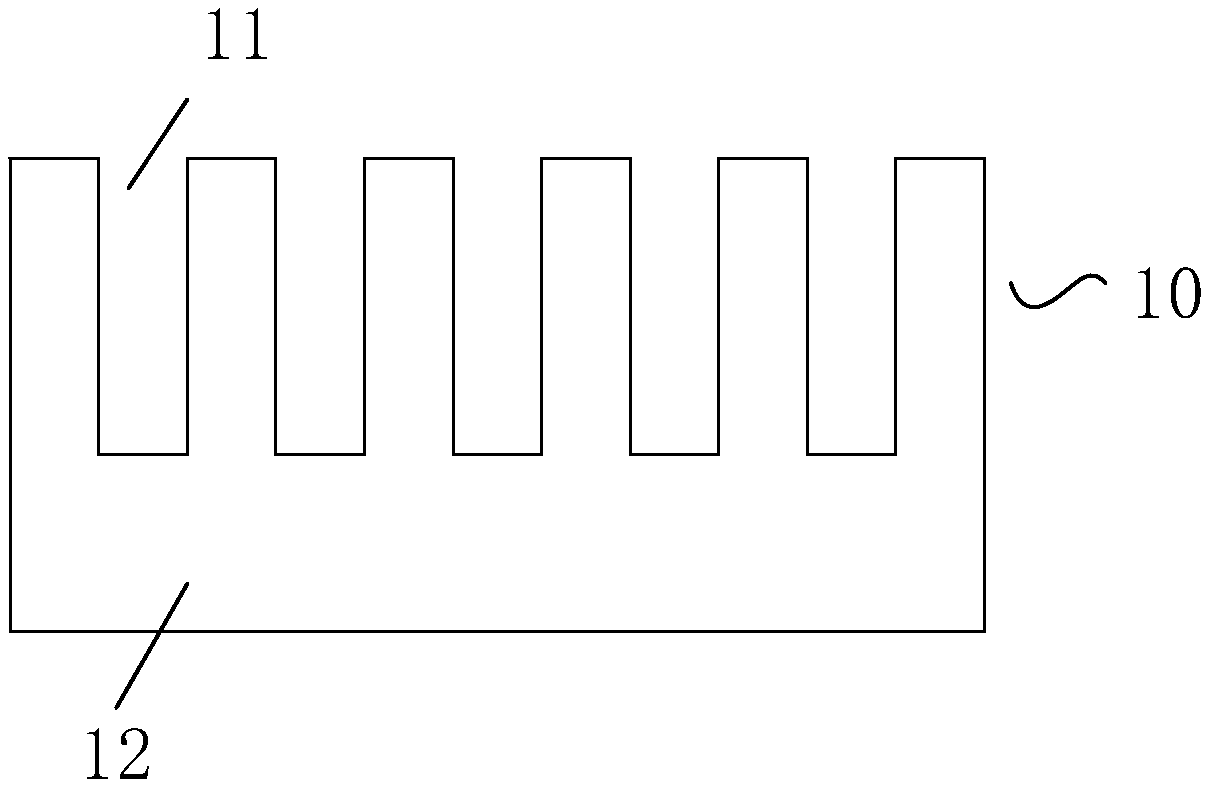
[0057] Provide a silicon substrate;

[0058] Using photolithography and plasma etching to dig a plurality of grooves with a width of 20nm (the distance between two adjacent grooves is 40nm) and a depth of 100nm on the silicon substrate, such as figure 1 shown;

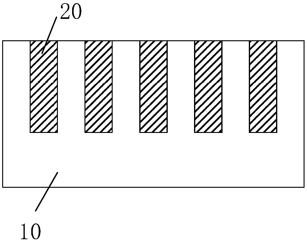
[0059] Using a thermal oxidation process, the substrate is thermally oxidized to form 1nm SiO 2 layer, and then use PECVD to deposit SiO in the groove 2 , and finally perform a CMP planarization process to form a similar figure 2 the structure shown;

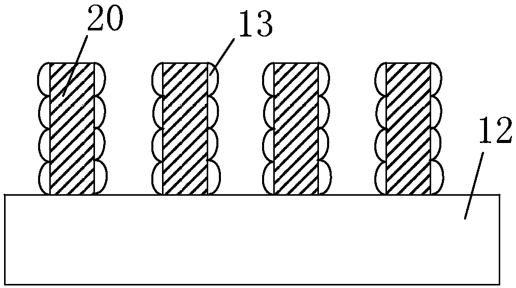
[0060] The second pre-nanowire is obtained by plasma alternate etching of anisotropic etching and isotropic etching, and the etching gas of anisotropic etching is SF 6 +O 2 , the etching gas for isotropic etching is SF 6 , the height of the second pre-nanowire is 3-6 nm;

[0061] Repeat the above process to obtain multiple stacked second pre-nanowires. For details, please refer to image 3 a ...


PUM


Abstract

The invention provides a device comprising nanowires and a production method of the device. The production method comprises the steps of (S1) providing a substrate with grooves; (S2) filling the grooves with an insulating material to form insulating parts, wherein the grooves correspond to the insulating parts one by one; and (S3) etching to remove parts of the substrate at two sides of the insulating parts, forming a plurality of stacked nanowires by the remaining substrate located at two side walls of the insulating parts and forming a first substrate body by the remaining substrate outsidethe nanowires, wherein the insulating parts are located on the surface of the first substrate body. The nanowires formed by using the production method are relatively perfect in lattices and the performance of the device is relatively good; and furthermore, according to the production method, the nanowires are attached to the insulating parts, that is to say, the insulating parts provide the nanowires with support, so that the nanowires can be produced very long and thin, the fracture problem is avoided and high density of the nanowires can be achieved.

Description

technical field [0001] The present application relates to the field of semiconductors, in particular, to a device including nanowires and a manufacturing method thereof. Background technique [0002] In advanced CMOS manufacturing, the combination of nanowire channel and ring gate has become a hot technology to solve the process below 5nm: [0003] One method is: grow a Si / GeSi stack on the substrate by means of epitaxial growth, and then selectively etch the GeSi therein to leave Si nanowires. The advantage is that the process is similar to the FinFet process, but the limitation is that the epitaxial process has more lattice defects than bulk silicon, especially after multi-layer alternating epitaxy, it is difficult to ensure that the crystal lattice of the epitaxial layer is perfect, so the device performance will be affected. [0004] Another method is to use the method of directly etching the silicon substrate (anisotropic etching and isotropic etching alternately) to f...

Claims


Application Information

Patent Timeline
Patent Type & Authority Applications(China)
IPC IPC(8): H01L27/092H01L29/10H01L21/8238H01L21/8252B82Y40/00
CPCB82Y40/00H01L21/823807H01L21/8252H01L27/092H01L29/1033
Inventor 李俊杰吴振华张青竹王文武
Owner INST OF MICROELECTRONICS CHINESE ACAD OF SCI
Why Eureka
Try Eureka