
Semiconductor structure and operation method thereof

Active Publication Date: 2018-12-04
MACRONIX INT CO LTD
View PDF4 Cites 0 Cited by
  • Summary
  • Abstract
  • Description
  • Claims
  • Application Information

AI Technical Summary

Problems solved by technology

However, the current only flows through the MOS surface with low on-state resistance, which makes the ESD discharge path limited and it is not easy to improve ESD performance
In addition, a MOS with a high breakdown voltage (Breakdown Voltage, BV) also has a high trigger voltage (Trigger Voltage), which increases the risk of MOS damage
In the field of power semiconductor components, the above two considerations are a great challenge in improving the effectiveness of ESD protection

Method used


Image

  • Semiconductor structure and operation method thereof
  • Semiconductor structure and operation method thereof
  • Semiconductor structure and operation method thereof

Examples


Embodiment Construction

[0052] The present invention will be described more fully with reference to the accompanying drawings of this embodiment. However, the present invention can also be embodied in various forms and should not be limited to the embodiments described herein. In the drawings, the thicknesses of layers and regions may be exaggerated for clarity. The same or similar symbols represent the same or similar elements, and the following paragraphs will not repeat them one by one.

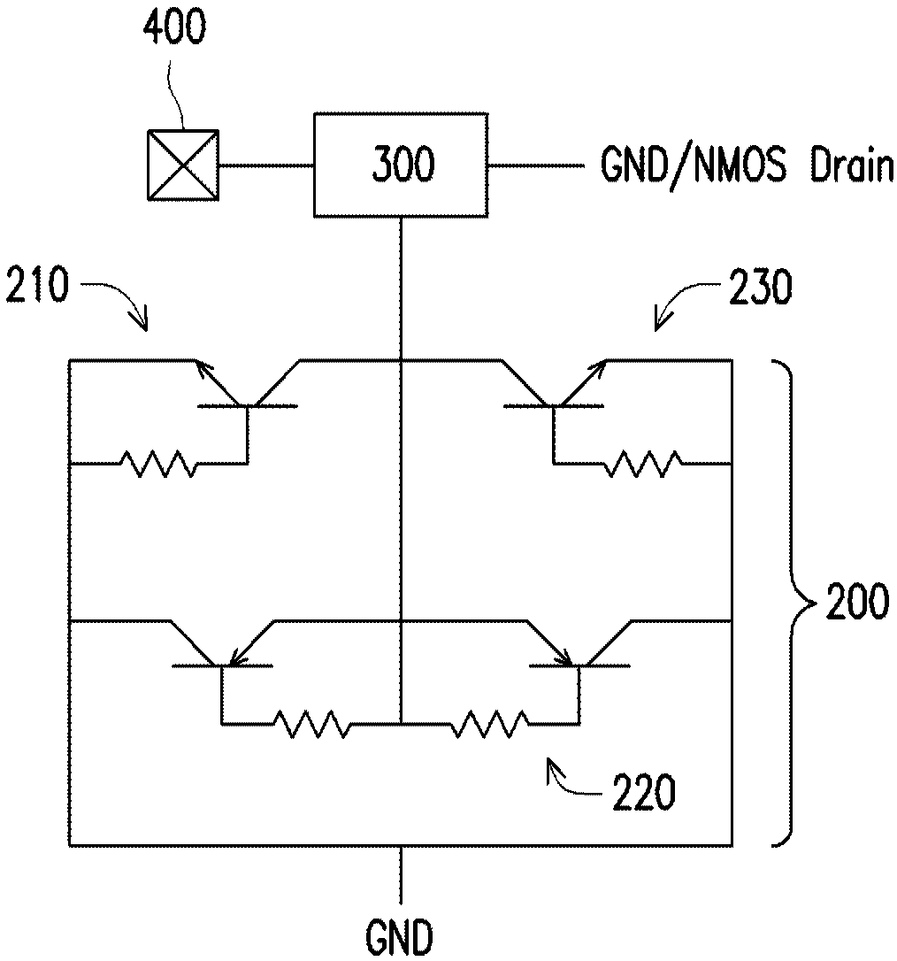
[0053] figure 1 is an equivalent circuit diagram of a semiconductor structure according to an embodiment of the present invention.

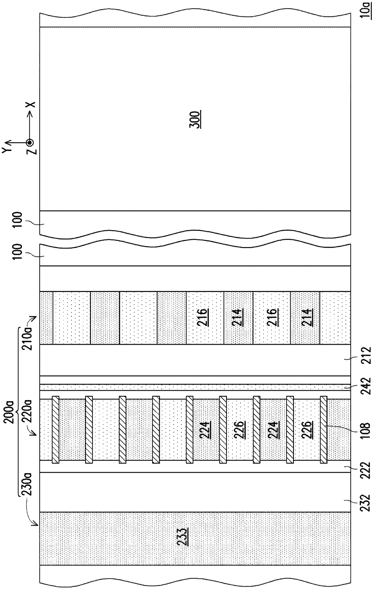
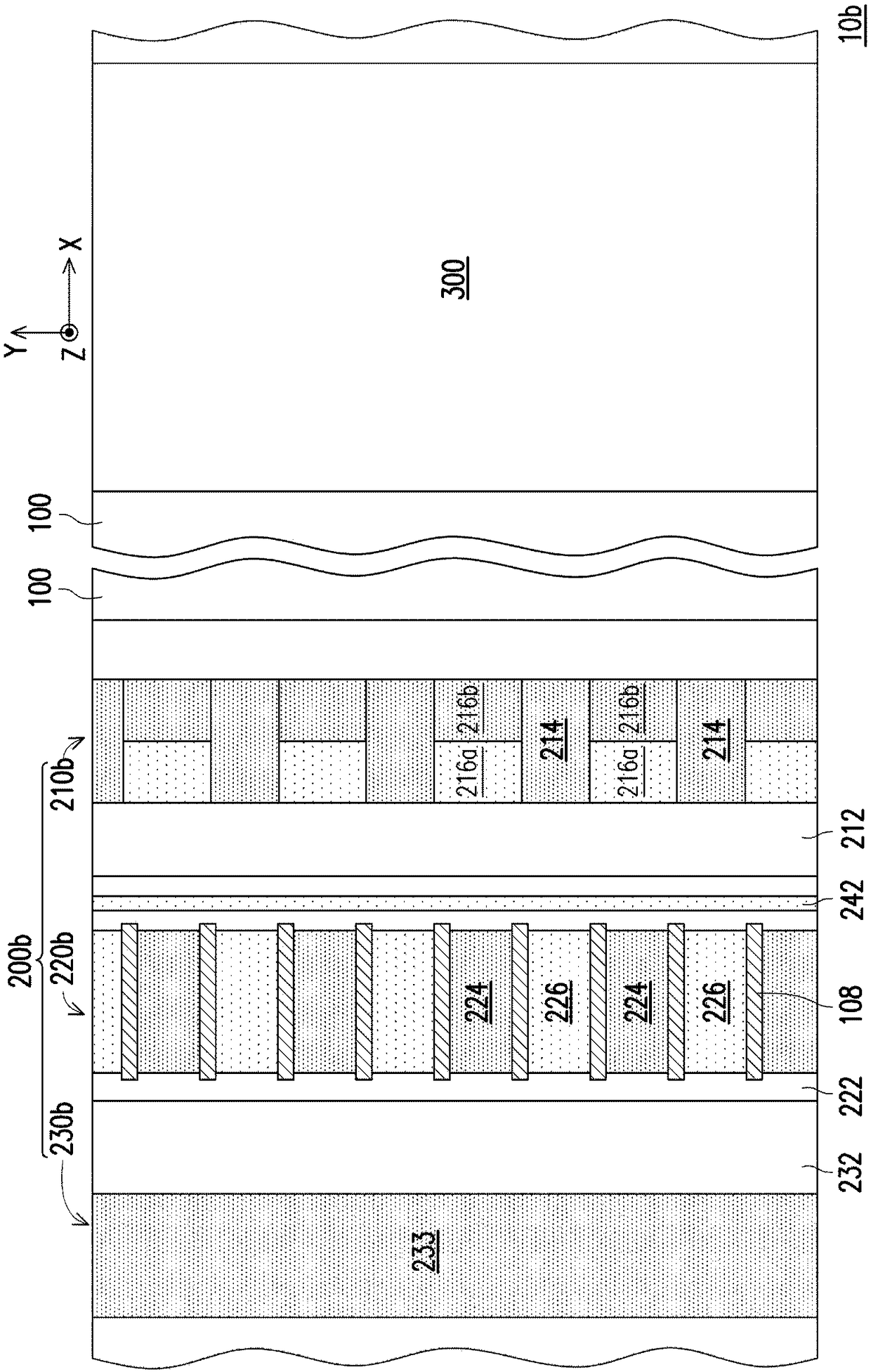
[0054] Please refer to figure 1 , the present embodiment provides a semiconductor structure 1 including an ESD protection element 200 and a semiconductor element 300 . The ESD protection device 200 is located between the semiconductor device 300 and a ground terminal GND. In detail, the ESD protection element 200 includes a first guard ring 210 , a second guard ring 220 and a t...


PUM


Abstract

A semiconductor structure includes a first guard ring and a second guard ring. The first guard ring is positioned in the substrate. The first guard ring includes a plurality of first doped regions anda plurality of second doped regions that are all arranged alternately. The first doped regions and the second doped regions are mutually different in conductivity types. The second guard ring is positioned beside the first guard ring. The second guard ring includes a plurality of third doped regions, a plurality of fourth doped regions and a plurality of mask layers, wherein the third doped regions and the fourth doped regions are alternately arranged. All of the third doped regions correspond to all of the second doped regions through one to one correspondence. All of the fourth doped regions correspond to all of the first doped regions through one to one correspondence. The third doped regions and the first doped regions are the same in conductivity type and are arranged in a staggered.The mask layers are respectively disposed on the substrate between the third doped regions and the fourth doped regions.

Description

technical field [0001] The present invention relates to a semiconductor structure and its operation method, and in particular to a semiconductor structure with electrostatic discharge (ElectroStatic Discharge, ESD) protection capability and its operation method. Background technique [0002] Electrostatic discharge (ESD) is a phenomenon in which charge accumulates on a non-conductor or an ungrounded conductor, and then travels rapidly and discharges in a short period of time through the discharge path. Electrostatic discharge can cause damage to circuits in integrated circuits. For example, a human body, a machine for packaging integrated circuits, or an instrument for testing integrated circuits are all common charged objects. When the above-mentioned charged objects come into contact with the chip, it is possible to discharge the chip. The instantaneous power of electrostatic discharge can cause damage or failure of the integrated circuits in the chip. [0003] Because i...

Claims


Application Information

Patent Timeline
Patent Type & Authority Applications(China)
IPC IPC(8): H01L23/60H01L27/02
CPCH01L23/60H01L27/0251H01L27/0292H01L27/0296
Inventor 陈永初
Owner MACRONIX INT CO LTD
Features
  • Generate Ideas
  • Intellectual Property
  • Life Sciences
  • Materials
  • Tech Scout
  • Unparalleled Data Quality
  • Higher Quality Content
  • 60% Fewer Hallucinations
Learn More