Semiconductor structure, memory structure and manufacturing method thereof

A memory and semiconductor technology, applied in the manufacture of semiconductor/solid-state devices, semiconductor devices, electric solid-state devices, etc., can solve the problems of easy offset of conductive plugs, high contact resistance of conductive plugs, and small effective contact area

Active Publication Date: 2018-12-04
CHANGXIN MEMORY TECH INC
View PDF8 Cites 17 Cited by
  • Summary
  • Abstract
  • Description
  • Claims
  • Application Information

AI Technical Summary

Problems solved by technology

With the development of technology, the size of the DRAM shrinks, and the feature size and cell area of ​​the DRAM decrease accordingly, which makes it easy for the formed conductive plug to shift, so that the conductive plug The effective contact area between the plug and the active region in the semiconductor substrate becomes smaller, so that the contact resistance between the conductive plug and the active region and the resistance of the conductive plug itself are relatively large

Method used


Image

  • Semiconductor structure, memory structure and manufacturing method thereof
  • Semiconductor structure, memory structure and manufacturing method thereof
  • Semiconductor structure, memory structure and manufacturing method thereof

Examples


Embodiment 1

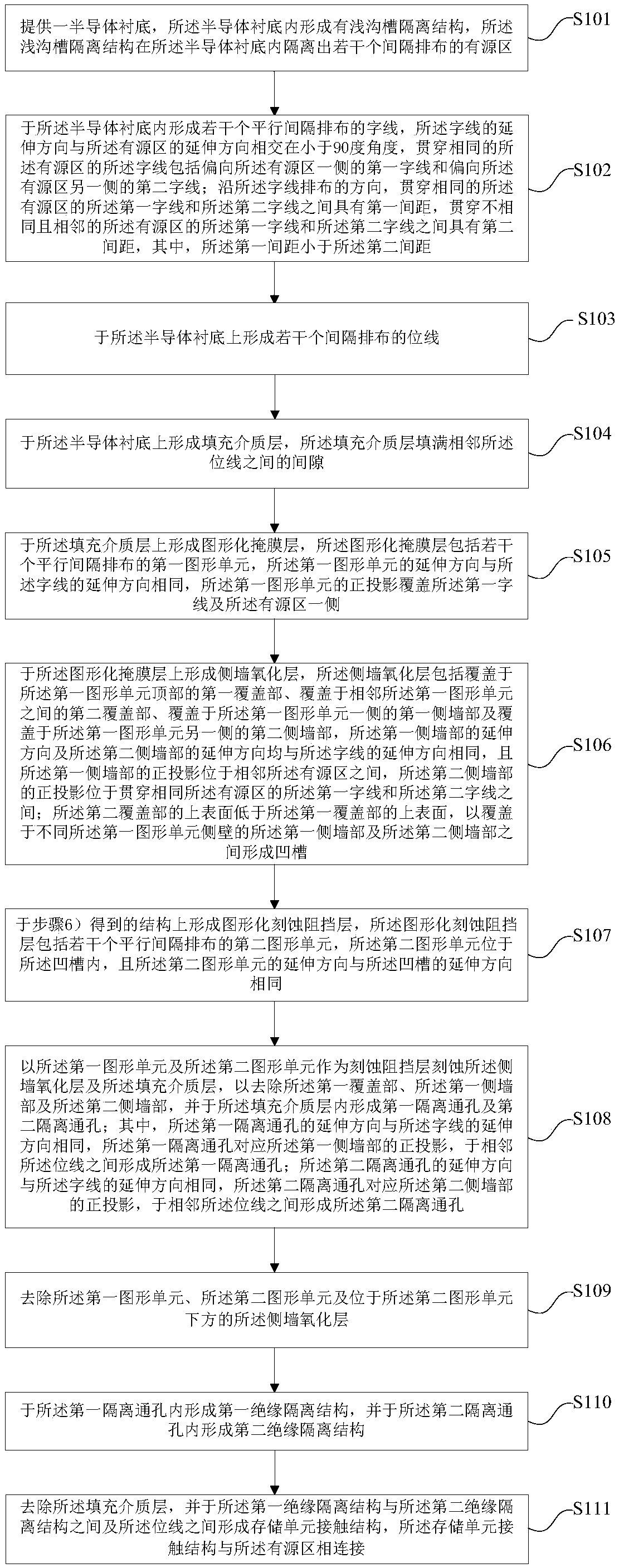
[0244] Such as figure 1 Shown, the present invention provides a kind of preparation method of memory structure, and the preparation method of described memory structure comprises the following steps:

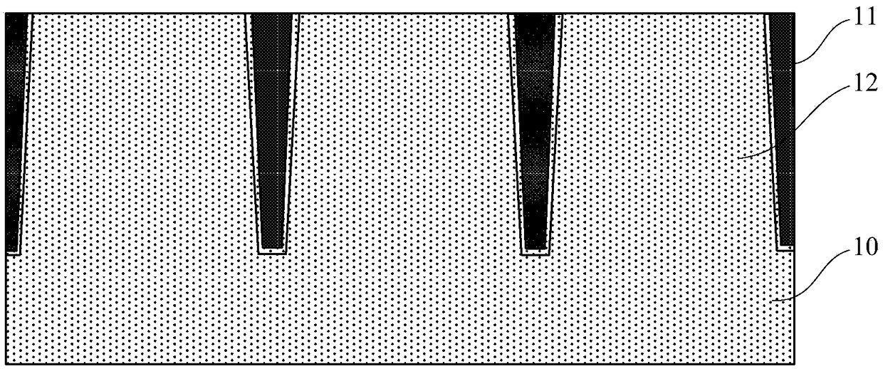
[0245] 1) A semiconductor substrate is provided, and a shallow trench isolation structure is formed in the semiconductor substrate, and the shallow trench isolation structure isolates several active regions arranged at intervals in the semiconductor substrate;

[0246] 2) A plurality of word lines arranged in parallel and at intervals are formed in the semiconductor substrate, the extension direction of the word lines intersects with the extension direction of the active region at an angle less than 90 degrees, and runs through the same active region. The word lines in the region include a first word line biased to one side of the active region and a second word line biased to the other side of the active region; along the direction in which the word lines are arranged, the same...

Embodiment 2

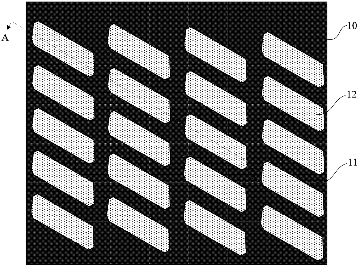
[0319] Please combine Figure 2 to Figure 24 read on Figure 25 to Figure 26 The present invention also provides a memory structure, which includes: a semiconductor substrate 10, a shallow trench isolation structure 11 is formed in the semiconductor substrate 10, and the shallow trench isolation structure 11 is formed on the semiconductor substrate Several active regions 12 arranged at intervals are isolated in the bottom 10; several word lines 13 are arranged at intervals in parallel, and the word lines 13 are located in the semiconductor substrate 10, and the extending direction of the word lines 13 is in line with that of the semiconductor substrate 10. The extending directions of the active regions 12 intersect at an angle of less than 90 degrees; the word lines 13 running through the same active region 12 include the first word lines 13a biased to one side of the active region 12 and the second word line 13b biased to the other side of the active region 12; along the dir...

Embodiment 3

[0339] see Figure 27 , the present invention also provides a method for preparing a semiconductor structure, the method for preparing a semiconductor structure comprising the following steps:

[0340] 1) providing a semiconductor substrate, a shallow trench isolation structure is formed in the semiconductor substrate, and the shallow trench isolation structure isolates several active regions arranged at intervals in the semiconductor substrate;

[0341] 2) forming several parallel and spaced protruding structures on the semiconductor substrate, the upper surface of the protruding structures is higher than the upper surface of the semiconductor substrate; the extension direction of the bit line is the same as the active the directions of extension of the zones intersect at a first angle less than 90 degrees;

[0342] 3) forming a side wall structure on the side wall of the bit line, and the side wall structure covers the outer wall of the bit line;

[0343] 4) forming a fill...


PUM


Abstract

The invention provides a semiconductor structure, a memory structure and a manufacturing method thereof. The method comprises the following steps: 1) a semiconductor substrate is provided; 2) a word line is formed in the semiconductor substrate; 3) a bit line is formed on the semiconductor substrate; 4) a filling dielectric layer is formed on the semiconductor substrate; 5) a graphical mask layeris formed on the filling dielectric layer; 6) a side wall oxide layer is formed on the graphical mask layer; 7) a graphical etching barrier layer is formed on the structure obtained in the step 6); 8)a first isolation through hole and a second isolation through hole are formed in the filling dielectric layer; 9) a first graphical unit, a second graphical unit and a side wall oxide layer below thesecond graphical unit are removed; 10) a first insulation isolation structure is formed in the first isolation through hole, and a second insulation isolation structure is formed in the second isolation through hole; and 11) the filling dielectric layer is removed, and a conductive plug is formed. The conductive plug can realize reduction of contact resistance between the conductive plug and an active region.

Description

technical field [0001] The invention belongs to the technical field of integrated circuit manufacturing, and in particular relates to a semiconductor structure, a memory structure and a preparation method thereof. Background technique [0002] With the development of technology, the size of the conductive plug used to electrically connect the functional devices in the semiconductor substrate with the outside in the semiconductor structure is getting smaller and smaller, so that the conductive plug is prone to offset, and the conductive plug and the active region The effective contact area becomes smaller, for example, Dynamic Random Access Memory (Dynamic Random Access Memory, DRAM for short) is composed of many repeated storage units. Each memory cell is mainly composed of a transistor and a capacitor controlled by the transistor. Each transistor includes a gate and a source and drain located in the substrate. The source / drain is connected to the bit line. , and the drain / ...

Claims


Application Information

Patent Timeline
Patent Type & Authority Applications(China)
IPC IPC(8): H01L27/108H01L21/8242
CPCH10B12/34H10B12/488H10B12/482
Inventor 不公告发明人
Owner CHANGXIN MEMORY TECH INC
Why Eureka
Try Eureka