Manufacture method for COB packaged optoelectronic chip with side protection

A technology of photoelectric chips and manufacturing methods, which is applied in the manufacture of circuits, electrical components, final products, etc., can solve problems such as high cost and complicated process, and achieve the effect of reducing product cost, simple process, and large market application prospects

Active Publication Date: 2018-12-07
ANHUI SCI & TECH UNIV
View PDF8 Cites 8 Cited by
  • Summary
  • Abstract
  • Description
  • Claims
  • Application Information

AI Technical Summary

Problems solved by technology

[0003] At present, the MPPC device of Hamamatsu in Japan and the SiPM of SensL in Ireland adopt the method of converging the signal to the center of the device, and use photolithography, dry etching (or laser ablation) and other methods to break through the SiPM in the center of the de

Method used


Image

  • Manufacture method for COB packaged optoelectronic chip with side protection
  • Manufacture method for COB packaged optoelectronic chip with side protection
  • Manufacture method for COB packaged optoelectronic chip with side protection

Examples


Embodiment Construction

[0033] Below in conjunction with accompanying drawing, the present invention is described in further detail by embodiment:

[0034] A method for manufacturing a COB package photoelectric chip with side protection, specifically comprising the following steps:

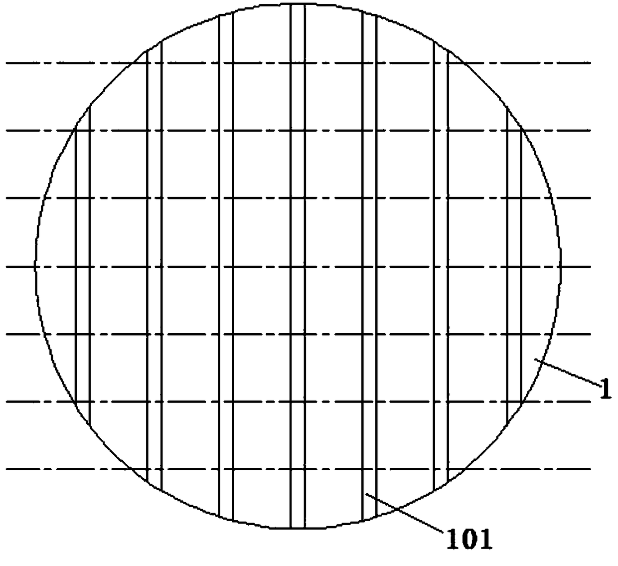
[0035] 1). Prepare the wafer optoelectronic device 1 and PCB board 2 to be processed. The front and back of the wafer optoelectronic device 1 are provided with electrodes, which are the front electrode and the back electrode respectively;

[0036] 2).See figure 1 , half-cut the electrode surface of the wafer optoelectronic device 1, and use a dicing machine to cut along the longitudinal scribing lane reserved on the surface of the front electrode of the wafer optoelectronic device 1 to 1 / 2 of the thickness of the wafer optoelectronic device 1. The width of the cutting groove 101 is between 200-300 microns;

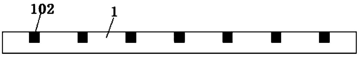
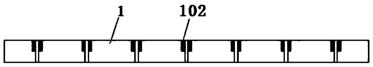
[0037] 3). See figure 2 Inject the insulating potting compound 102 into the cutting groove 101, requiring the ...


PUM


Abstract

The invention discloses a manufacture method for a COB packaged optoelectronic chip with side protection. According to the manufacture method, a COB packaged optoelectronic chip can be obtained through the cutting of a wafer optoelectronic device, the insulating treatment of a side surface, COB package, electrode connection and finished product cutting. Two side surfaces of the COB packaged optoelectronic chip manufactured by the method of the invention are protected by an insulating adhesive, and therefore, it can be ensured that conductive silver paste does not contact the silicon of the side surfaces of the chip, a condition that a front electrode and the back electrode of the chip are short circuited can be prevented. The method is simple in process, can realize automatic production, can greatly reduce product cost, and has a very bright market application prospect.

Description

Technical field: [0001] The invention relates to the production field of photoelectric chips, in particular to a method for manufacturing a COB packaged photoelectric chip with side protection. Background technique: [0002] Silicon photomultipliers are often used in imaging applications. It is necessary to splice a single SiPM device into a large-scale array on four sides. The traditional method of bonding wires will cause a wide gap "dead zone" on the side where the bonding electrodes are located (for optical signals Insensitive), since SiPM is mostly used in weak light detection, high detection efficiency is very important in use. Therefore, in the package of the SiPM, it is necessary to increase the proportion of the effective detection area as much as possible. [0003] At present, the MPPC device of Hamamatsu in Japan and the SiPM of SensL in Ireland adopt the method of converging the signal to the center of the device, and use photolithography, dry etching (or laser ...

Claims


Application Information

Patent Timeline
IPC IPC(8): H01L31/18H01L31/0203
CPCH01L31/0203H01L31/1876Y02P70/50
Inventor 韩意张远兵陈佩简兴朱立政
Owner ANHUI SCI & TECH UNIV
Why Eureka
Try Eureka