Supercharge Your Innovation With Domain-Expert AI Agents!

Photoelectric conversion device

A technology of a photoelectric conversion device and a photoelectric conversion module, which is applied in the field of carbon nanotubes, can solve the problems that cannot be realized and can not change the chirality of carbon nanotubes arbitrarily, and achieve the effect of increasing output power

Active Publication Date: 2018-12-07
TSINGHUA UNIV +1
View PDF5 Cites 0 Cited by
  • Summary
  • Abstract
  • Description
  • Claims
  • Application Information

AI Technical Summary

Problems solved by technology

[0004] However, it is still not possible to directly grow semiconducting carbon nanotubes with higher purity.
At the same time, in the prior art, the chirality of carbon nanotubes cannot be arbitrarily changed during the growth of carbon nanotubes, that is, carbon nanotubes cannot form carbon nanotubes with alternating semiconducting carbon nanotube segments and metallic carbon nanotube segments as required during the growth process. nanotube
At the same time, it is impossible to apply the above-mentioned carbon nanotubes with alternating semiconducting carbon nanotube segments and metallic carbon nanotube segments to carbon nanotube structures and applications of carbon nanotube structures, such as thin film transistors, photodetectors, Photoelectric conversion module, etc.

Method used


Image

  • Photoelectric conversion device
  • Photoelectric conversion device
  • Photoelectric conversion device

Examples


Embodiment Construction

[0028] The preparation of the carbon nanotube hand provided by the present invention and the carbon nanotube structure obtained by the method, the thin film transistor prepared by using the carbon nanotube structure, the photodetector, and the photoelectric conversion device will be further detailed in conjunction with specific examples below. illustrate.

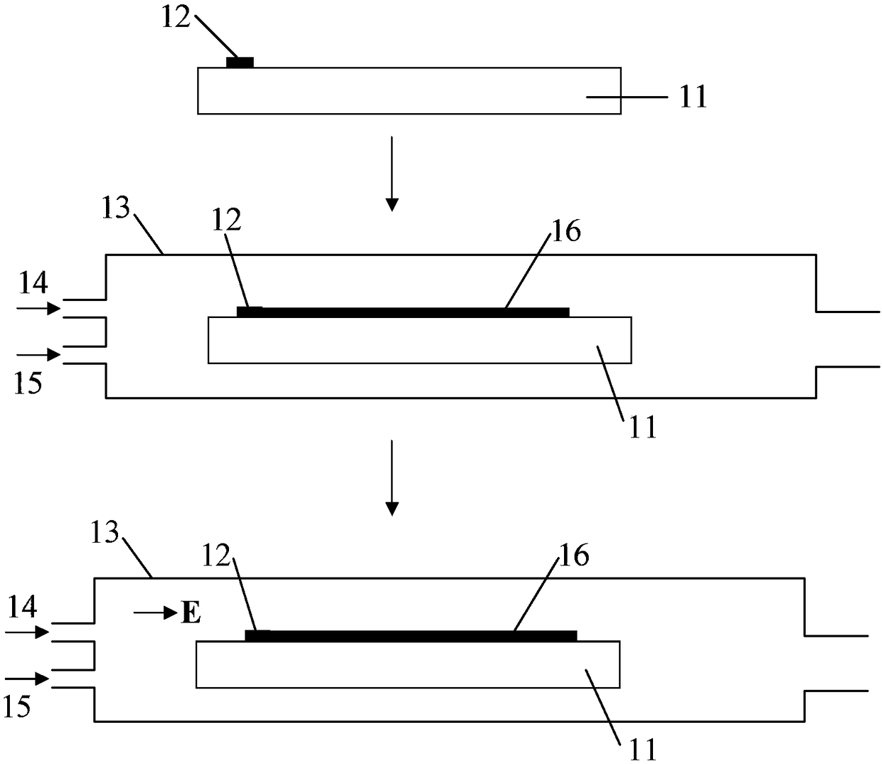
[0029] see figure 1 , the first embodiment of the present invention provides a method for preparing carbon nanotubes, which includes the following steps:

[0030] Step S11, providing a substrate 11, depositing a catalyst layer 12 on the surface of the substrate 11;

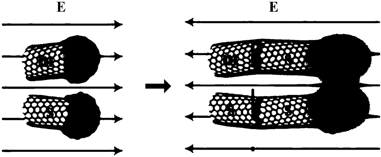
[0031] Step S12, setting the substrate 11 in a reaction furnace 13, heating to make the temperature in the reaction furnace reach a predetermined temperature, passing a carbon source gas 14 and a protective gas 15 into the reaction furnace 13, so that the substrate 11 Growing a carbon nanotube segment structure 16, the carbon nanotube segment structure 16 inc...


PUM

PropertyMeasurementUnit
Diameteraaaaaaaaaa

Abstract

The invention relates to a photoelectric conversion device which comprises a photoelectric conversion module. The photoelectric conversion module comprises a carbon nanotube structure and a coverage structure, the carbon nanotube structure comprises at least one carbon nanotube, the carbon nanotube comprises a semiconductor type carbon nanotube segment and two metallic carbon nanotube segments connected to the two ends of the semiconductor type carbon nanotube segment respectively, and the coverage structure covers part of the semiconductor type carbon nanotube segment, namely a coverage area.

Description

technical field [0001] The invention relates to the technical field of carbon nanotubes, in particular to a photoelectric conversion device prepared by using carbon nanotubes. Background technique [0002] Carbon nanotubes have attracted extensive attention due to their excellent properties such as high Young's modulus, tensile strength, and high thermal conductivity. [0003] In the single-walled carbon nanotubes prepared by the traditional chemical vapor deposition method, the ratio of metallic carbon nanotubes and semiconducting carbon nanotubes is about 1:2. In order to obtain semiconducting carbon nanotubes with higher purity, in the past two decades, after continuous research on the thermodynamics and kinetics of carbon nanotubes, people have been able to grow semiconducting carbon with a purity of 97% by CVD. nanotube. [0004] However, it is still not possible to directly grow semiconducting carbon nanotubes with higher purity. At the same time, in the prior art, ...

Claims


Application Information

Patent Timeline
IPC IPC(8): H01L51/30H01L51/46H01L51/05H01L51/42H01L35/24
CPCH10N10/856H10K85/221H10K10/466H10K30/451H10K10/82B82Y30/00Y02E10/549H10K10/484H10K30/65H01L31/022475H01L31/0481
Inventor 王江涛柳鹏姜开利范守善
Owner TSINGHUA UNIV
Features
  • R&D
  • Intellectual Property
  • Life Sciences
  • Materials
  • Tech Scout
  • Unparalleled Data Quality
  • Higher Quality Content
  • 60% Fewer Hallucinations
Learn More