

QLED (Quantum dot Light-Emitting Diode) device and preparation method thereof
A technology of devices and electron transport layers, which is applied in the field of QLED devices and its preparation, can solve problems such as effective carrier injection, reduced migration, and impact on device light extraction efficiency and service life, so as to promote electron transmission, improve efficiency and stability The effect of reducing the contact resistance
- Summary
- Abstract
- Description
- Claims
- Application Information
AI Technical Summary
Problems solved by technology
Method used
Image

Examples
Embodiment approach
[0036] As an embodiment, the preparation method of the QLED device includes the following steps:
[0037] S01. An anode substrate is provided, and a quantum dot light-emitting layer is prepared on the anode substrate;
[0038] S02. Prepare an electron transport layer of 4H-SiC material on the quantum dot light-emitting layer;
[0039] S03. preparing a metal buffer layer on the electron transport layer;
[0040] S04. Prepare a cathode on the metal buffer layer.
[0041] In the above step S01, the selection of the anode substrate is as described above, and in order to save space, details are not repeated here. The method for preparing the anode substrate can prepare an anode such as an ITO film on the substrate by magnetron sputtering. Specifically, the cleaned substrate is placed in a magnetron sputtering machine for ITO coating.
[0042]Further, the preparation of the quantum dot luminescent layer on the anode substrate can be realized by methods such as spin coating, prin...
Embodiment 1
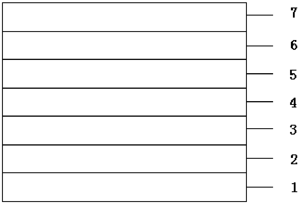
[0060] A QLED device comprising an ITO anode, a hole injection layer (PEDOT:PSS, thickness 50nm) combined on the anode, a hole transport layer (poly-TPD, thickness 30nm) combined on the hole injection layer, and a hole injection layer (poly-TPD, thickness 30nm) combined on the hole Quantum dot light-emitting layer (20nm) on the hole transport layer, electron transport layer (4H-SiC, thickness 30nm) combined on the quantum dot light-emitting layer, metal buffer layer (W, thickness 10nm) combined on the electron transport layer, And a cathode (silver, thickness 70nm) disposed on the metal buffer layer.
[0061] The preparation method of the QLED device comprises the following steps:
[0062] The 4H-SiC film is sputtered by radio frequency with 4H-SiC target, the sputtering process is: power 60W, sputtering pressure 0.6Pa, argon flow 50sccm, sputtering time 5min, thickness about 30nm;
[0063] The metal W was prepared by DC sputtering. The sputtering process was as follows: the ...
Embodiment 2
[0065] A QLED device comprising an ITO anode, a hole injection layer (PEDOT:PSS, thickness 50nm) combined on the anode, a hole transport layer (poly-TPD, thickness 30nm) combined on the hole injection layer, and a hole injection layer (poly-TPD, thickness 30nm) combined on the hole Quantum dot light-emitting layer (20nm) on the hole transport layer, electron transport layer (4H-SiC, thickness 130nm) combined on the quantum dot light-emitting layer, metal buffer layer (Ni, thickness 30nm) combined on the electron transport layer, And a cathode (silver, thickness 70nm) disposed on the metal buffer layer.
[0066] The preparation method of the QLED device comprises the following steps:
[0067] 4H-SiC thin film is sputtered by radio frequency with 4H-SiC target, the sputtering process is: power 60W, sputtering pressure 0.6Pa, argon flow 50sccm, sputtering time 15min, thickness about 130nm;
[0068] Metal Ni was prepared by DC sputtering, the sputtering process was as follows: sp...
PUM
 Abstract
Description
Claims
Application Information