

Organic electroluminescent device and preparation method
An electroluminescent device and luminescent technology, which is applied in the manufacture of organic semiconductor devices, electric solid devices, semiconductor/solid state devices, etc., can solve the problems of total reflection loss, low light extraction performance, poor refractive index, etc.
- Summary
- Abstract
- Description
- Claims
- Application Information
AI Technical Summary
Problems solved by technology
Method used
Image

Examples
preparation example Construction
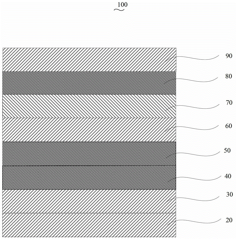
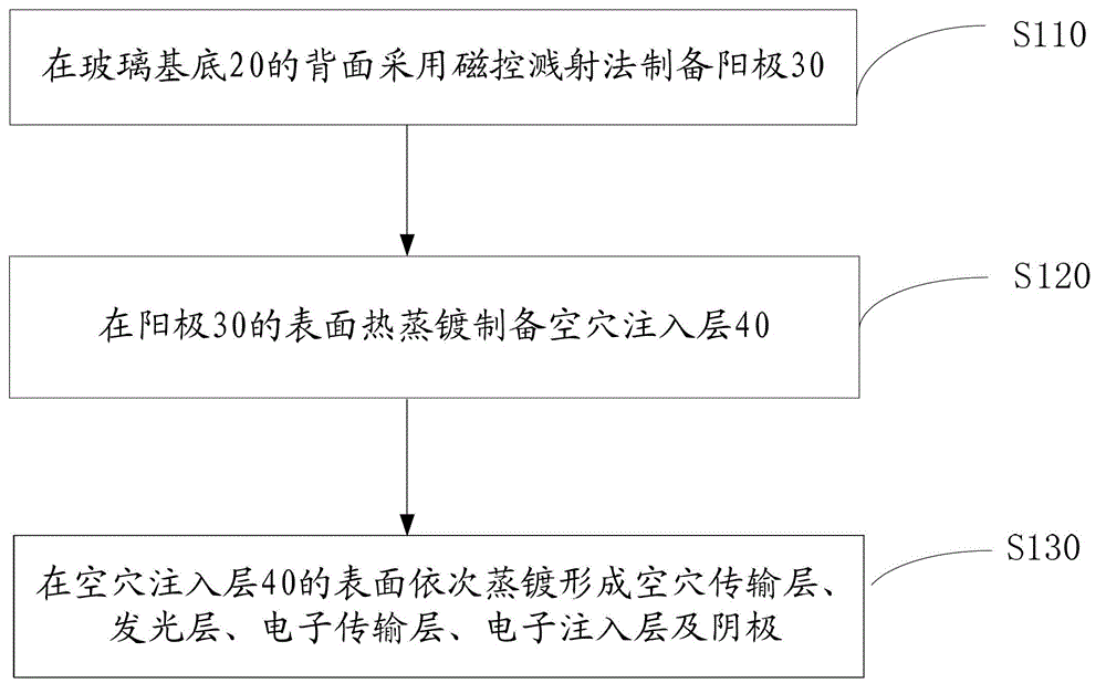
[0033] Please also see figure 2 , the preparation method of the organic electroluminescent device 100 of an embodiment, it comprises the following steps:
[0034] Step S110 , preparing the anode 30 on the back of the glass substrate 20 by magnetron sputtering.
[0035] The glass substrate 20 is glass with a refractive index of 1.8-2.2, and the transmittance at 400 nm is higher than 90%. The glass substrate 20 is preferably glass with a grade of N-LAF36, N-LASF31A, N-LASF41A or N-LASF44.
[0036] The material of the anode 30 includes at least one of indium tin oxide (ITO), aluminum zinc oxide (AZO) and indium zinc oxide (IZO). The thickness of the anode 30 is 80nm~300nm. A preferred thickness is 120 nm.
[0037] Magnetron sputtering at a vacuum pressure of 5×10 -5 Pa~2×10 -3 Under Pa, the acceleration pressure is 300V-800V, the magnetic field is 50G-200G, and the power density is 1W / cm 2 ~40W / cm 2 .
[0038] In this embodiment, the glass substrate 20 is rinsed with di...
Embodiment 1
[0052] The structure prepared in this example is / glass substrate / ITO / CuO:F4-TCNQ:PrO 2 / TCTA / Alq 3 / Bphen / CsF / Ag organic electroluminescence device.
[0053] The glass substrate is N-LASF44. After rinsing the glass substrate with distilled water and ethanol, soak it in isopropanol for one night. The anode is prepared on the surface of the glass substrate by magnetron sputtering, the anode material is ITO, the thickness is 120nm, and the condition of magnetron sputtering is that the pressure is 8×10 -4 Pa, accelerating voltage 400V, magnetic field 100G, power density 25W / cm 2 , using electron beams to prepare a hole injection layer on the surface of the anode, the material of the hole injection layer is CuO and F4-TCNQ doped in PrO 2 Among them, CuO accounts for PrO 2 The mass percentage is 20%, F4-TCNQ accounts for PrO 2 The mass percentage is 0.5%, and the electron beam is used at a pressure of 8×10 -4 Pa, the energy density is 20W / cm 2 The hole injection layer was pr...
Embodiment 2
[0058]The structure prepared in this example is / glass substrate / AZO / Ag 2 O:1T-NATA:Pr 2 o 3 / TAPC / ADN / TAZ / LiF / Pt organic electroluminescent devices.
[0059] The glass substrate is N-LAF36. After rinsing the glass substrate with distilled water and ethanol, soak it in isopropanol for one night; prepare an anode on the surface of the glass substrate by magnetron sputtering. The anode material is AZO with a thickness of 300nm , the condition of magnetron sputtering is that the pressure is 2×10 -3 Pa, acceleration voltage 300V, magnetic field 50G, power density 1W / cm 2 , using electron beams to prepare a hole injection layer on the surface of the anode, the material of the hole injection layer is Ag 2 O and 1T-NATA doped in praseodymium trioxide, where Ag 2 O accounts for 10% of the mass percentage of praseodymium dioxide, 1T-NATA accounts for 0.1% of the mass percentage of praseodymium dioxide, and the electron beam is used at a pressure of 2×10 -3 Pa, the energy density ...
PUM
| Property | Measurement | Unit |
|---|---|---|
| Thickness | aaaaa | aaaaa |
| Power density | aaaaa | aaaaa |
| Thickness | aaaaa | aaaaa |
Abstract
Description
Claims
Application Information