Perovskite photovoltaic cells passivated with au@cds nanoparticles

A nanoparticle and photovoltaic cell technology, applied in the field of materials, can solve problems such as unfavorable carrier migration and low carrier mobility, and achieve the effects of improving battery short-circuit current and filling factor, inhibiting diffusion, and accelerating migration.

Active Publication Date: 2022-07-19
WUHAN INSTITUTE OF TECHNOLOGY
View PDF4 Cites 0 Cited by
  • Summary
  • Abstract
  • Description
  • Claims
  • Application Information

AI Technical Summary

Problems solved by technology

However, although the chemical properties of insulator SiO2 are stable, it is not conducive to carrier migration; TiO 2 There are defects such as high temperature sintering and low carrier mobility

Method used


Image

  • Perovskite photovoltaic cells passivated with au@cds nanoparticles
  • Perovskite photovoltaic cells passivated with au@cds nanoparticles
  • Perovskite photovoltaic cells passivated with au@cds nanoparticles

Examples


Embodiment 1

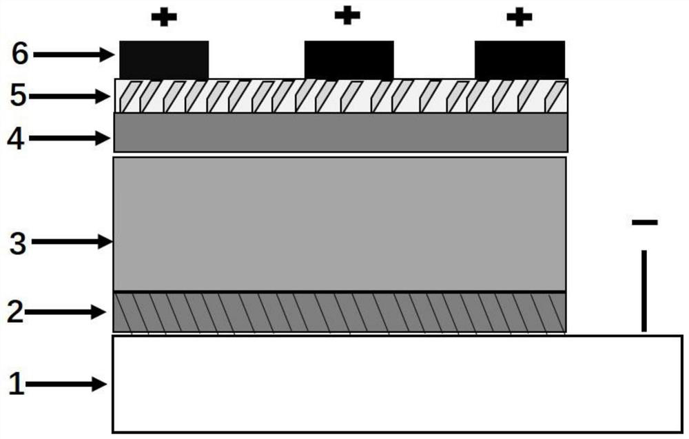
[0038] like figure 1 As shown, a planar structure perovskite photovoltaic cell includes a transparent conductive substrate, an electron transport layer, a perovskite photosensitive active layer, an interface passivation layer, a hole transport layer and a metal electrode, and its preparation method includes the following steps:

[0039] (1) Treatment of transparent conductive substrate: cleaning FTO (fluorine-doped SnO 2 ) conductive glass sheet, first soak the conductive glass sheet in a solution containing detergent (such as Libai brand liquid detergent) for 30 minutes, then repeatedly scrub and rinse with clean water; then polish with polishing powder; then separately Put it into a vessel containing deionized water, acetone and alcohol for 20 minutes respectively; finally, put it in deionized water to rinse twice, dry it with a nitrogen gun and put it in an oven to dry at 80°C;

[0040] (2) SnO 2 QD Thin Film Preparation: SnO on FTO Substrate 2 The QD film was placed in ...

Embodiment 2

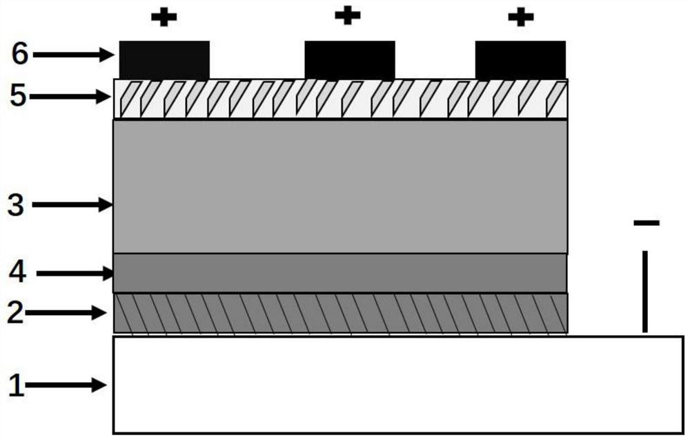
[0052] like figure 1 As shown, a planar structure perovskite photovoltaic cell includes a transparent conductive substrate, an electron transport layer, a perovskite photosensitive active layer, an interface passivation layer, a hole transport layer and a metal electrode, and its preparation method includes the following steps:

[0053] (1) cleaning ITO conductive glass sheet: same as Example 1;

[0054] (2) SnO 2 Thin Film Preparation: Preparation of SnO on ITO Substrate 2 The thin film was placed in a UV-ozone cleaner, and treated with UV-ozone for 15 minutes in an atmospheric atmosphere and room temperature, and the treated SnO 2 / The ITO substrate was quickly transferred into the glove box;

[0055] (3) Preparation of perovskite photosensitive active layer: the same as in Example 1;

[0056] (4) Preparation of interface passivation layer on perovskite photosensitive film:

[0057] a. Solution preparation: The previously synthesized Au@CdS nanoparticles with Au partic...

Embodiment 3

[0063] like figure 1 As shown, a planar structure perovskite photovoltaic cell includes a transparent conductive substrate, an electron transport layer, a perovskite photosensitive active layer, an interface passivation layer, a hole transport layer and a metal electrode, and its preparation method includes the following steps:

[0064] (1) Cleaning the FTO conductive glass sheet: the same as in Example 1;

[0065] (2) SnO 2 QD film preparation: same as Example 1;

[0066] (3) Preparation of perovskite photosensitive active layer: the same as in Example 1;

[0067] (4) Preparation of interface passivation layer on perovskite photosensitive film:

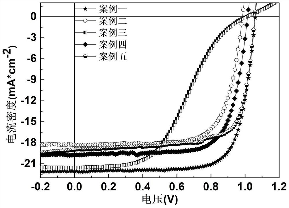
[0068]a. Solution preparation: The previously synthesized Au@CdS nanoparticles with Au particle size of 30 nm and CdS coating thickness of 10 nm were dissolved in 1 ml of chlorobenzene solvent, ultrasonicated in an ultrasonic cleaner for 1 h, and the solution concentration was 0.03 mmol / mL. stand-by;

[0069] b. Preparation of i...


PUM

PropertyMeasurementUnit
thicknessaaaaaaaaaa
thicknessaaaaaaaaaa

Abstract

The invention discloses a perovskite photovoltaic cell passivated with Au@CdS nanoparticles. An interface passivation layer is arranged between the electron transport layer and the perovskite photoactive layer; or an interface passivation layer is arranged between the perovskite photoactive layer and the hole transport layer; or the electron transport layer and the perovskite photoactive layer are arranged An interface passivation layer is simultaneously arranged between the active layer and the hole transport layer; the interface passivation layer is a coating of Au@CdS nanoparticles with a core-shell structure. Effectively suppress its diffusion in the device (reduce leakage), reduce the interface barrier, achieve effective energy level matching between the hole / electron transport layer and the perovskite photosensitive layer, and balance the hole transport layer and the electron transport layer to their respective carriers. The current extraction rate, so as to achieve the purpose of improving the battery short-circuit current and fill factor.

Description

technical field [0001] The invention belongs to the technical field of materials, and specifically relates to a perovskite photovoltaic cell. Background technique [0002] Until 2018, the highest efficiency of perovskite photovoltaic cells has exceeded 23% (Solar cell efficiencytable, https: / / www.nrel.gov / pv / assets / images / efficiency-chart-20180716.jpg), in the process of commercial development , stability is of great concern. In order to improve the efficiency and stability of battery devices, in addition to preparing high-quality perovskite photoactive layers, proper interface modification and passivation (including electron / hole transport interface layer preparation, doping and related interface modification, etc.) It is very important in the process of device fabrication and research. [0003] At present, many achievements on interface modification and passivation of perovskite photoactive layers have been reported at home and abroad (Adv. Mater. 2019, 31: e1805702). T...

Claims


Application Information

Patent Timeline
Patent Type & Authority Patents(China)
IPC IPC(8): H01L51/42H01L51/44
CPCH10K30/10H10K30/00H10K30/88Y02E10/549
Inventor 秦平力吴彤王正春余雪里马良熊伦陈相柏
Owner WUHAN INSTITUTE OF TECHNOLOGY
Why Eureka
Try Eureka