photosensitive element

A photosensitive element and nanohole array technology, applied in the field of photosensitive elements, can solve the problem that the sensitivity of the photosensitive element is not very high, etc.

Inactive Publication Date: 2017-01-25
NANKAI UNIV
View PDF4 Cites 0 Cited by
  • Summary
  • Abstract
  • Description
  • Claims
  • Application Information

AI Technical Summary

Problems solved by technology

However, the sensitivity of traditional semiconductor photosensitive elements is not very high

Method used


Image

  • photosensitive element
  • photosensitive element
  • photosensitive element

Examples


Embodiment 1

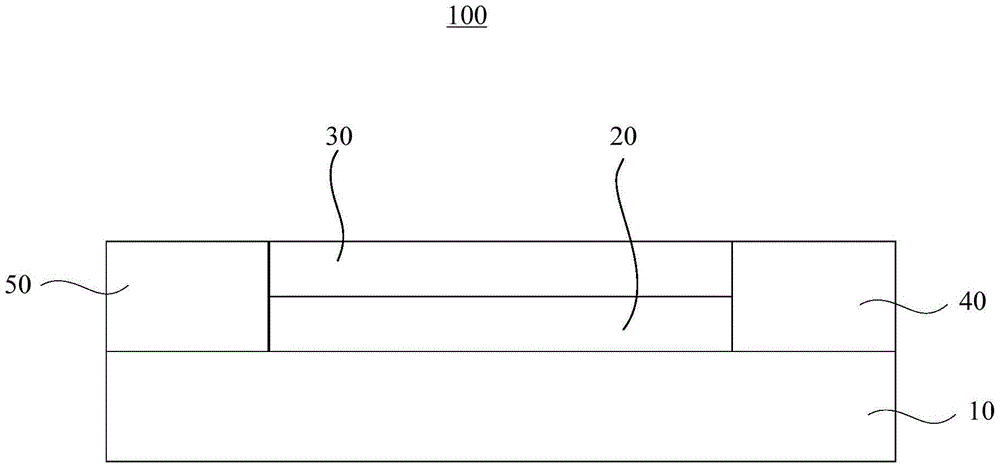
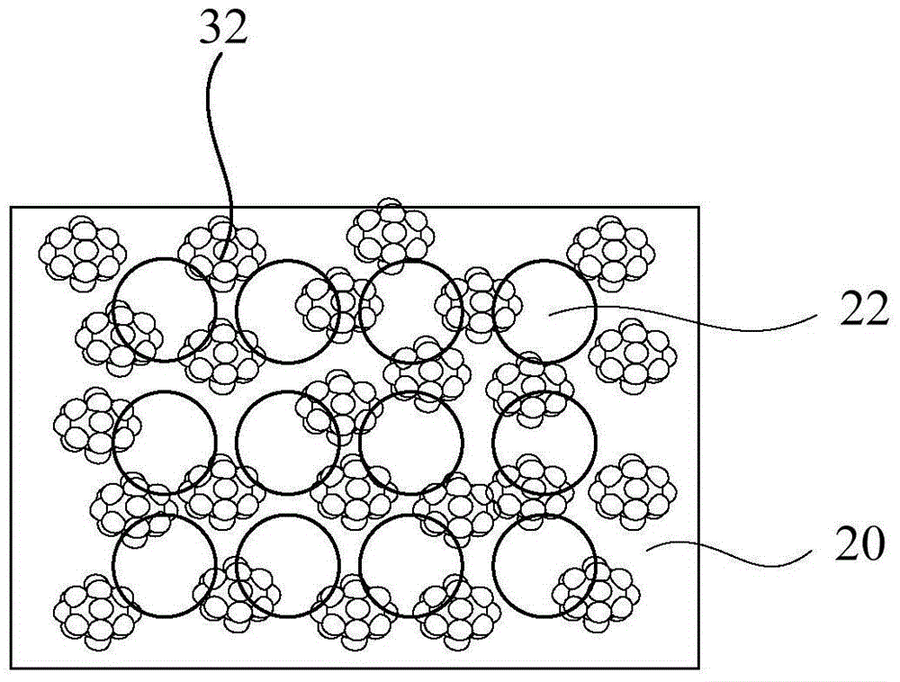
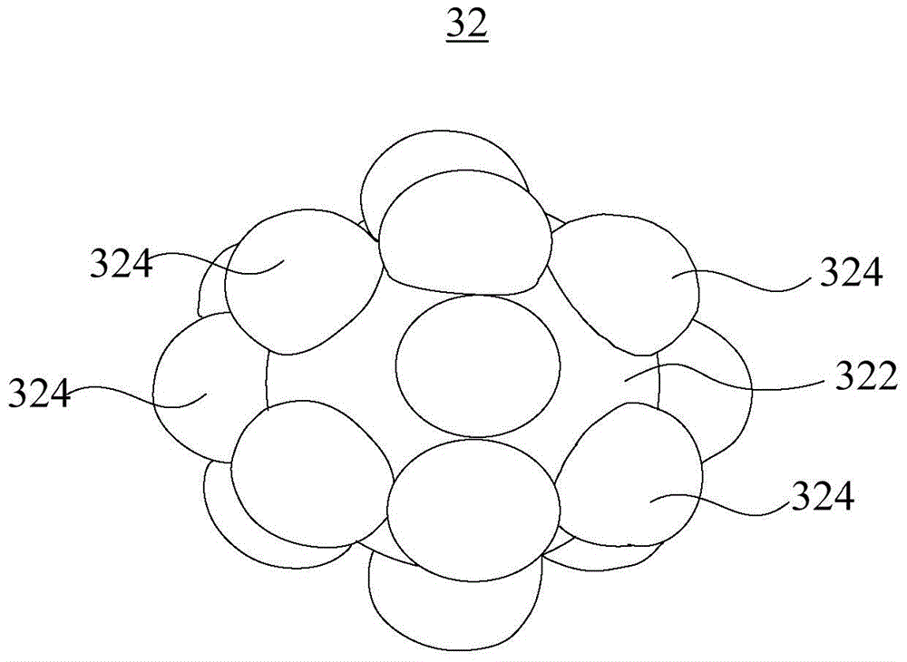
[0036] The photosensitive element I is prepared, and the photosensitive element I includes a semiconductor active layer, a nanohole array layer, a submicron particle layer, an anode and a cathode. Wherein the material of the semiconductor active layer is silicon. The diameter of the nanoholes in the nanohole array layer is 350 nm, the thickness of the nanohole array layer is 50 nm, and the distance between adjacent nanoholes is 100 nm. The material of the nanohole array layer is silver. The submicron particle layer is formed from submicron silver particles. The submicron silver particles include central silver nanoparticles with a diameter of 200nm and 18 surrounding silver nanoparticles with a diameter of 100nm protruding from the surface of the central silver nanoparticles. Both anode and cathode materials are silver.

[0037] Light with a wavelength of 700nm to 1600nm is irradiated onto the photosensitive element I from the side of the submicron particle layer, and the l...

Embodiment 2

[0039] The photosensitive element II was prepared, and the structure of the photosensitive element II was basically the same as that of the photosensitive element I in Example 1. The difference is that, in the photosensitive element II, a layer of spherical silver nanoparticles with a particle diameter of 100nm is stacked above the nanohole array layer instead of a submicron silver particle layer.

[0040] When light with a wavelength of 700nm-1600nm is irradiated from the side of the spherical silver nanoparticle layer onto the photosensitive element II, the enhancement factor of the obtained photocurrent is as follows: Figure 5 shown. As can be seen from the figure, compared with Example 1, the spherical silver nanoparticles in the photosensitive element II can also enhance the photocurrent intensity of the semiconductor active layer under the light condition with a wavelength greater than 1200nm, however, its enhancement effect is not as good as that of the photosensitive ...

Embodiment 3

[0042] The photosensitive element III was prepared, and the structure of the photosensitive element III was basically the same as that of the photosensitive element I in Example 1. The difference is that, in the photosensitive element III, a layer of spherical silver nanoparticles with a particle diameter of 200nm is stacked above the nanohole array layer instead of a submicron silver particle layer.

[0043] Irradiate light with a wavelength of 700nm to 1600nm from one side of the spherical silver nanoparticle layer onto the photosensitive element III, and the enhancement factor of the obtained photocurrent is as follows: Figure 5 As can be seen from the figure, compared with Example 1, the spherical silver nanoparticles in the photosensitive element III can also enhance the photocurrent intensity of the semiconductor active layer under the light conditions with a wavelength greater than 950nm, however, its enhanced The effect is not as good as the submicron particle layer o...


PUM


Abstract

The invention discloses a photosensitive component. The photosensitive component comprises a semiconductor active layer, a nanopore array layer, a submicron particle layer, a positive electrode and a negative electrode, wherein the nanopore array layer is provided with nanopores which pass through the nanopore array layer and extend in the thickness direction of the nanopore array layer; the semiconductor active layer, the nanopore array layer and the submicron particle layer are sequentially stacked; two ends of the nanopore array layer are aligned to two ends of the submicron particle layer; the positive electrode and the negative electrode are arranged on the semiconductor active layer and are respectively arranged at two ends of the nanopore array layer and the submicron particle layer. According to the photosensitive component, when submicron particles are irradiated by incident light; by virtue of resonance of local surface plasmas generated by free electrons in the photosensitive component, the local electromagnetic fields on the surfaces of the submicron particles are greatly enhanced; by virtue of the resonant coupling effect of the local surface plasmas between the submicron particle structure and the nanopore array structure, the number of current carriers generated by a semiconductor is increased, so that the photocurrent intensity of the semiconductor is improved; the sensitivity is improved.

Description

technical field [0001] The invention relates to the technical field of optical devices, in particular to a photosensitive element. Background technique [0002] Infrared technology has the characteristics of good concealment, no electromagnetic interference, little environmental influence, strong detection ability and long range, so it has high application value in military and civilian fields. The forerunner of the development of infrared technology is the development of infrared detectors. Photon detectors with semiconductors as the core are the mainstream of infrared detectors, and semiconductor photosensitive elements are the core components of the detectors. At present, researchers at home and abroad improve the quantum efficiency from the aspects of semiconductor materials and processing technology. In recent years, research reports have shown that the surface plasmon optical properties of metal micro-nanostructures can enhance the light absorption of semiconductors, t...

Claims


Application Information

Patent Timeline
Patent Type & Authority Patents(China)
IPC IPC(8): H01L31/101
CPCH01L31/035227H01L31/101
Inventor 陈平卢亚宾李星赵东旭林列
Owner NANKAI UNIV
Why Eureka
Try Eureka