

A 3D NAND memory and a method for manufacturing that same
A 3D NAND and memory technology, applied in the direction of electric solid-state devices, semiconductor devices, electrical components, etc., can solve the problems of poor electrical performance, wide distribution, reliability problems, etc., and achieve the effect of good electrical performance
- Summary
- Abstract
- Description
- Claims
- Application Information
AI Technical Summary
Problems solved by technology
Method used
Image

Examples
Embodiment Construction
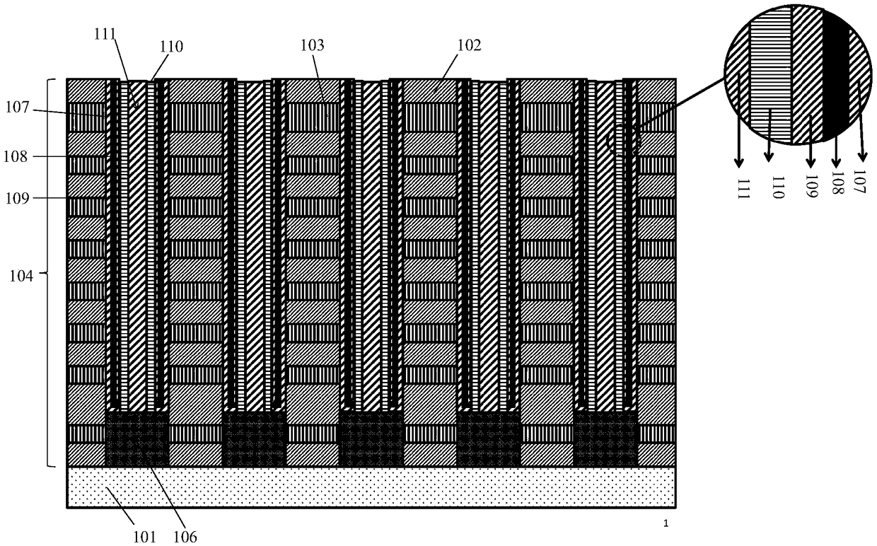
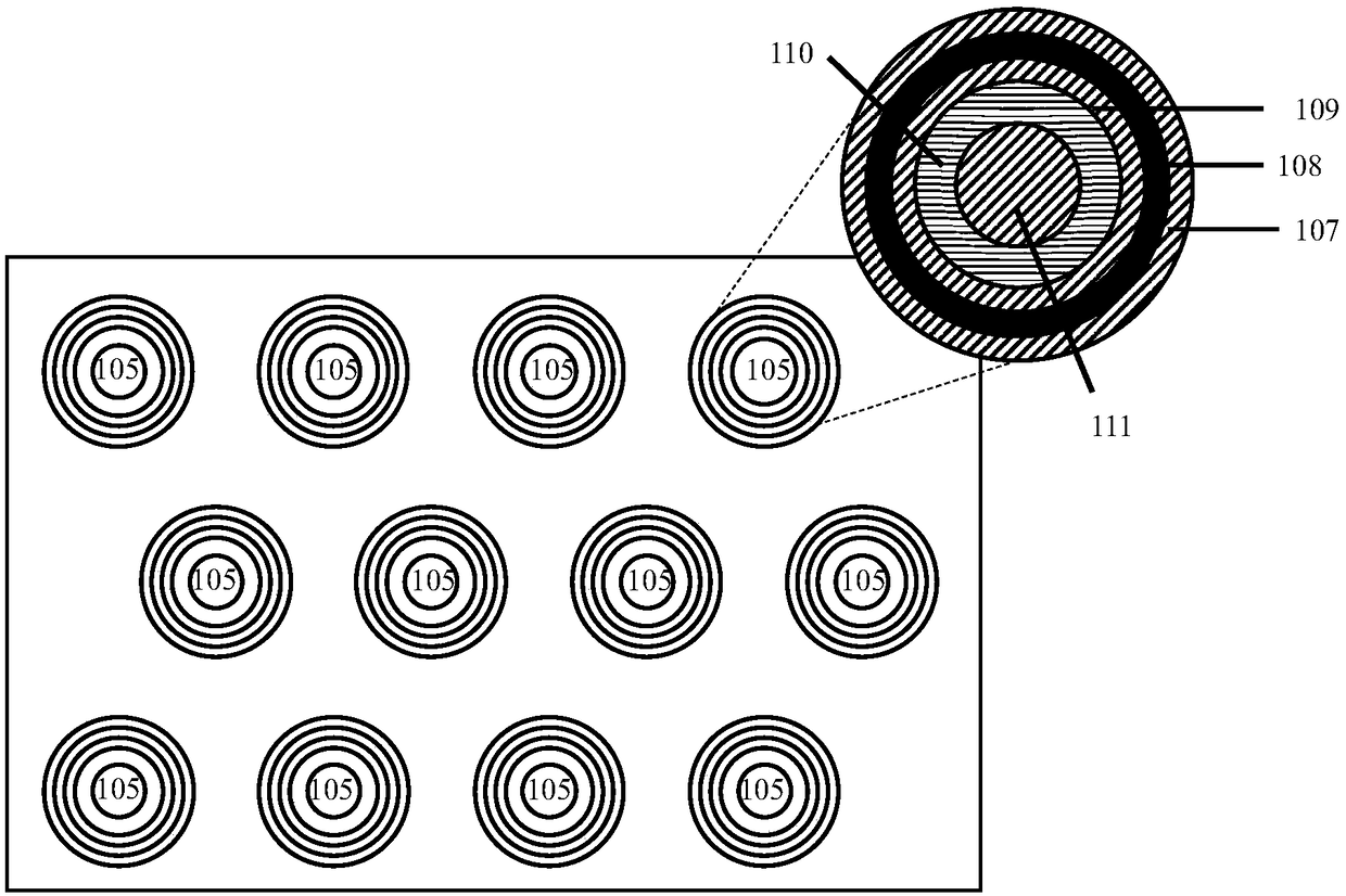
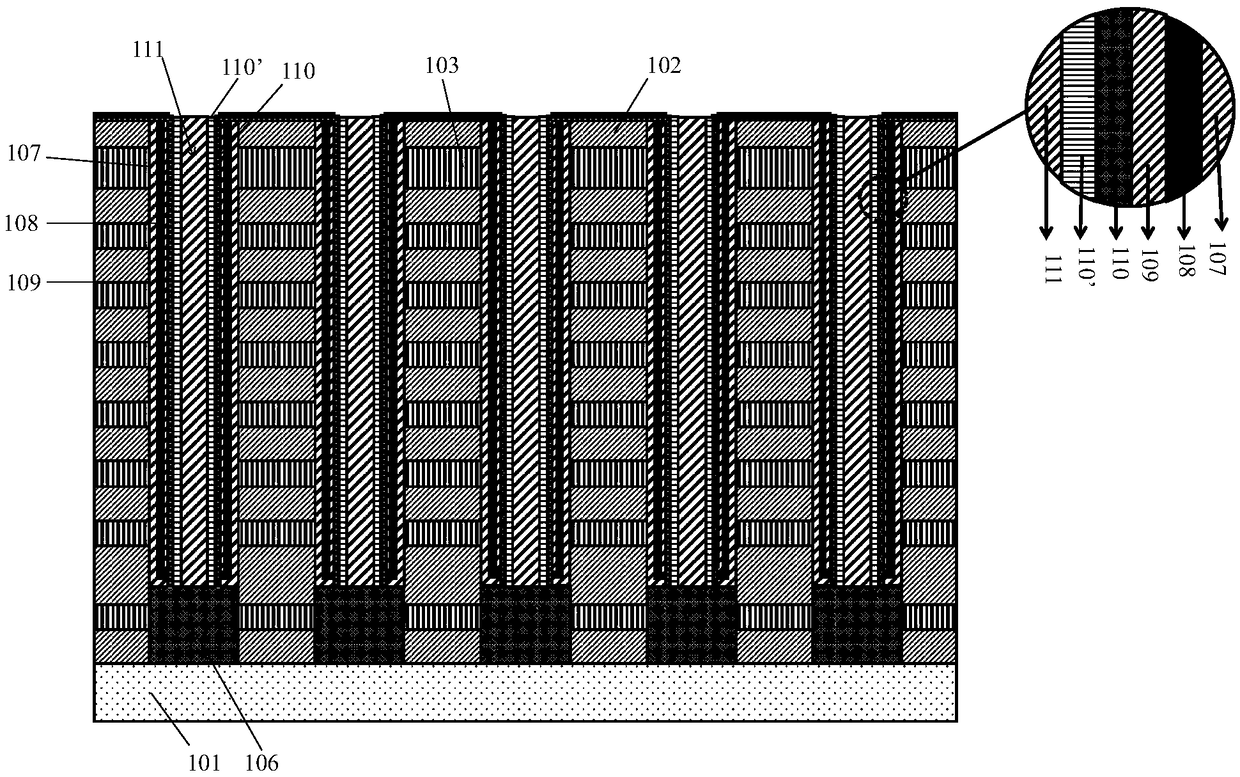
[0049] Based on the background technology, it can be seen that the existing 3D NAND memory has problems of poor electrical performance, for example, the on-state current is small and unstable, and the threshold voltage fluctuates greatly.
[0050] The inventors of the present application have discovered through research that the above-mentioned problems exist in the existing 3D NAND memory, because the existing 3D NAND memory mostly uses polysilicon material as the channel layer material in order to control the manufacturing cost.
[0051] However, polysilicon material is used as the channel layer, because there are crystal boundaries in polysilicon, so charge traps will be generated in the channel layer, so that as the number of word line stacked layers increases, the on-state current of the memory cell will decrease with the stacked layer. Rapidly decreasing numbers can lead to dyslexia.
[0052] When polysilicon material is used as the channel layer material, a larger on-st...
PUM
 Abstract
Description
Claims
Application Information