soi substrate, semiconductor device and method of forming the same

A semiconductor and substrate technology, applied in semiconductor devices, semiconductor/solid-state device manufacturing, electrical components, etc., can solve the problems of compromise design between speed and power consumption, limited applications, increased power consumption, etc., and achieve the purpose of suppressing self-heating effect, the effect of suppressing the floating body effect, and promoting the effect of the floating body effect

Active Publication Date: 2021-03-30
NINGBO SEMICON INT CORP
View PDF5 Cites 0 Cited by
  • Summary
  • Abstract
  • Description
  • Claims
  • Application Information

AI Technical Summary

Problems solved by technology

The floating body effect will not only reduce the gain of the device and lead to unstable operation of the device, but also reduce the leakage breakdown voltage and cause a single-transistor latch-up effect, resulting in a large off-state leakage current and increased power consumption
These will limit the application of the device in the circuit, especially making the compromise design of speed and power consumption more difficult

Method used


Image

  • soi substrate, semiconductor device and method of forming the same
  • soi substrate, semiconductor device and method of forming the same
  • soi substrate, semiconductor device and method of forming the same

Examples


Embodiment Construction

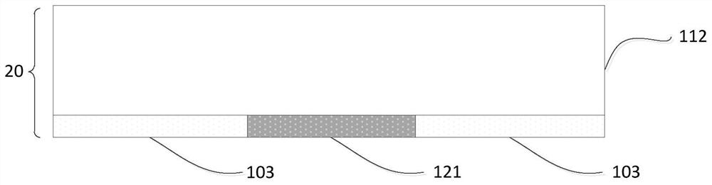
[0064] As mentioned above, in a common SOI structure, due to the isolation effect of the oxide layer, the top silicon layer is in an electrically floating state relative to the back substrate, resulting in a floating body effect, which affects the performance of the device. In addition, the isolation effect of the oxide layer also comes from heating effects. In view of this, the present invention provides an improved SOI structure, a semiconductor device using the SOI structure and a method for forming the same. According to an embodiment of the present invention, an embedded silicon layer is formed in the oxide layer of the SOI substrate, and a heavily doped silicon layer is formed at the bottom of the top silicon layer above the embedded silicon layer, the heavily doped silicon layer and the embedded silicon layer and the backside The substrate forms a PNP / NPN bipolar transistor, and the holes / electrons accumulated at the bottom of the top silicon can be exported by groundin...


PUM


Abstract

The invention discloses a SOI substrate, a semiconductor device and a forming method thereof. The SOI substrate includes: providing a first silicon substrate, the first silicon substrate including a first silicon layer; Providing a second silicon substrate, the second silicon substrate comprising a third silicon layer and an oxide layer, a surface of the oxide layer having grooves penetrating theoxide layer, the grooves being located in an active region, the grooves being filled with a silicon material of a different doping type than the first silicon layer, the third silicon layer being of the same doping type as the first silicon layer; Bonding one surface of the first silicon substrate and an oxide layer surface of the second silicon substrate to form the SOI substrate. The invention suppresses the self-heating effect and floating body effect of the SOI structure, and suppresses the self-heating effect of the SOI structure.

Description

technical field [0001] The present invention relates to the technical field of semiconductors, in particular to an SOI substrate, a semiconductor device and a method for forming the same. Background technique [0002] The full name of SOI is Silicon-On-Insulator, that is, silicon on an insulating substrate. This technology introduces an oxide layer between the top silicon layer and the back substrate. Compared with bulk silicon substrates, SOI substrates have the following advantages in device performance: reduced parasitic capacitance, lower power consumption, elimination of latch-up effects, and suppression of substrate pulse current interference. [0003] The performance of SOI is also affected by its own structure. Due to the low thermal conductivity of the oxide layer in the SOI structure, the heat generated by the device cannot be quickly released through the back substrate, and the continuously generated heat quickly accumulates in the active area, resulting in the "...

Claims


Application Information

Patent Timeline
Patent Type & Authority Patents(China)
IPC IPC(8): H01L21/762H01L29/06
CPCH01L21/762H01L29/06
Inventor 陈达
Owner NINGBO SEMICON INT CORP
Why Eureka
Try Eureka