A NAND Flash controller with an error detection and correction mechanism

An error detection and correction, controller technology, applied in the direction of instruments, static memory, etc., can solve the problems of improving, NAND Flash memory bit flip, not providing protection bit flip and so on

Inactive Publication Date: 2018-12-18
NORTHWESTERN POLYTECHNICAL UNIV
View PDF5 Cites 20 Cited by
  • Summary
  • Abstract
  • Description
  • Claims
  • Application Information

AI Technical Summary

Problems solved by technology

[0005] However, the more important thing is that the bit flipping phenomenon may occur during the frequent use of NAND Flash memory, especially as the single-chip capacity of NAND Flash memory is getting larger and larger, and the structure of the chip is becoming more and more complicated. The probability of bit flipping errors is increasing day by day, and commercial NAND Flash shelf products do not provide the ability to protect against bit flipping

Method used


Image

  • A NAND Flash controller with an error detection and correction mechanism
  • A NAND Flash controller with an error detection and correction mechanism
  • A NAND Flash controller with an error detection and correction mechanism

Examples


Embodiment Construction

[0039] The present invention will be further described below in conjunction with the accompanying drawings and embodiments, and the present invention includes but not limited to the following embodiments.

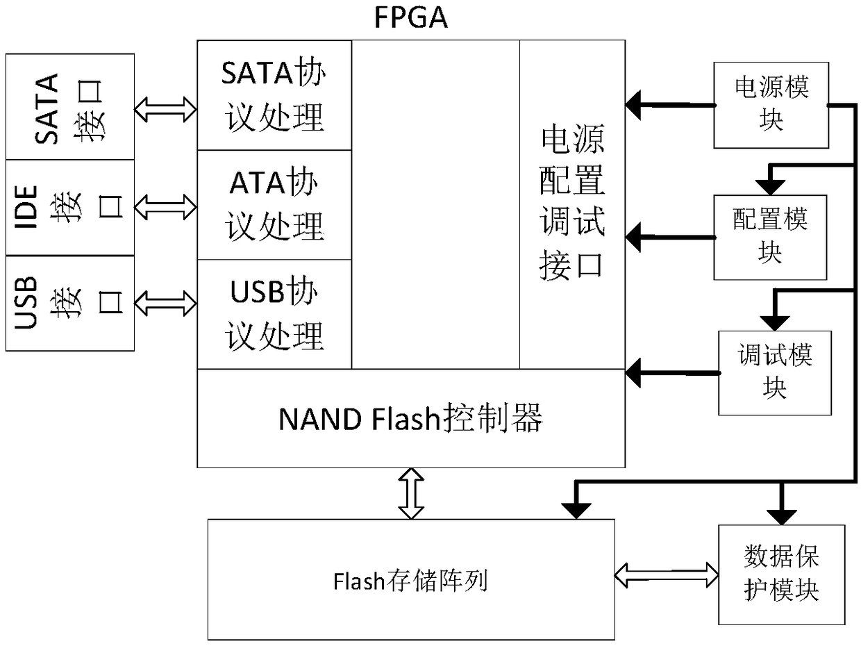
[0040] The present invention selects a NAND Flash chip with a capacity not less than 2GB to design the controller (here the NAND Flash chip K9F2G08U0A with a capacity of 2GB from SAMSUNG Company is used for illustration).

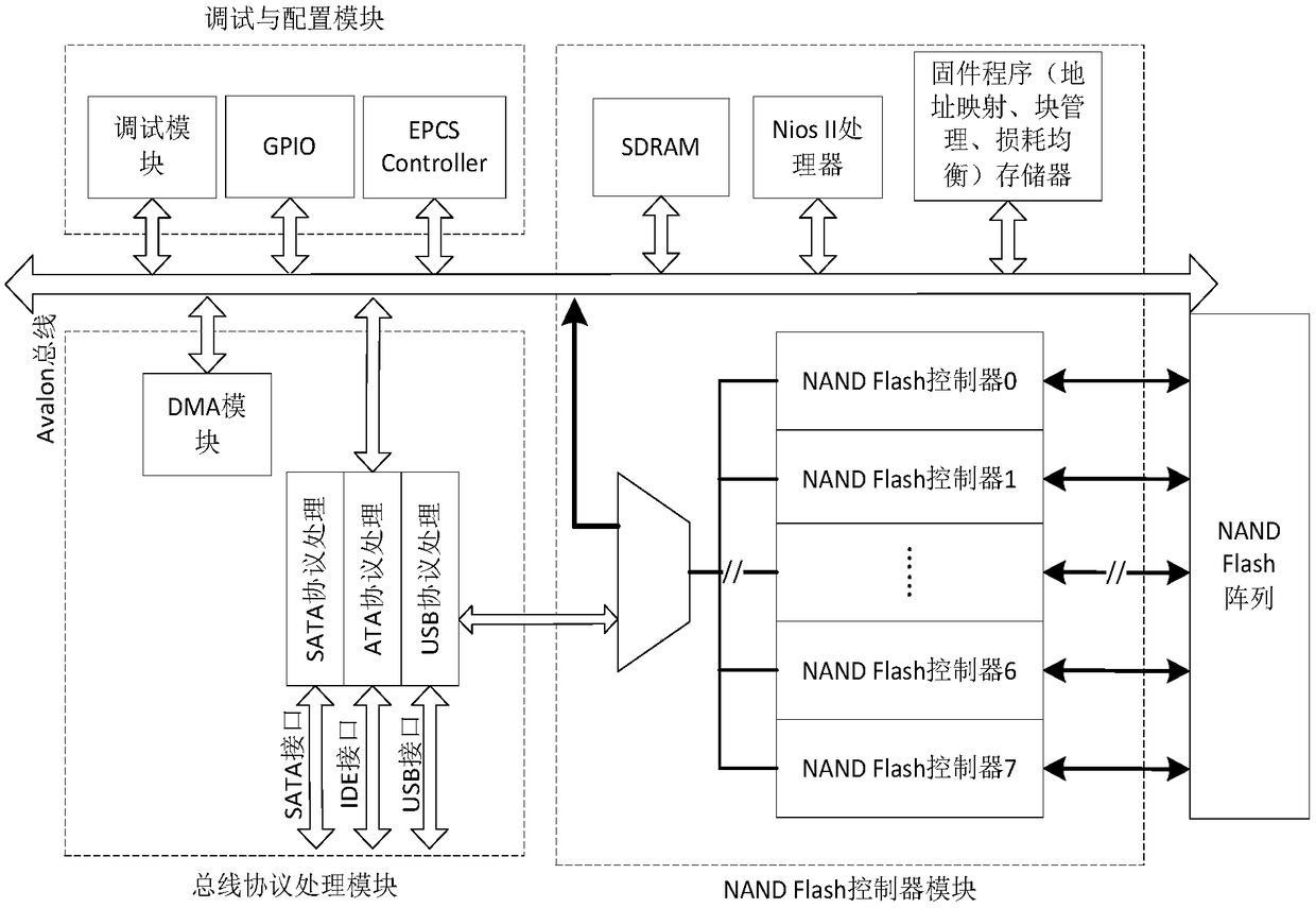
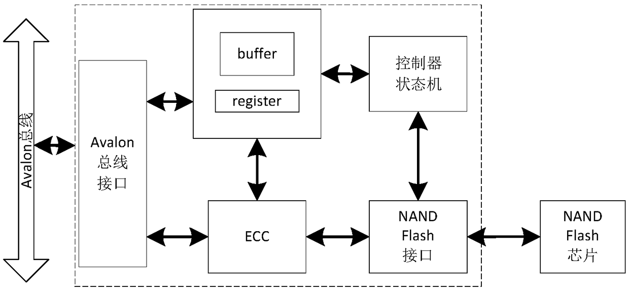
[0041] One end of the NAND Flash controller hardware module is connected to the NAND Flash chip, and the other end is connected to the processor bus in the system through the on-chip bus. The names and definitions of each signal connected to the Flash chip end are the same as those of the NAND Flash chip. The connection between the controller and the processor side adopts a method similar to the SRAM interface. The interface description of the NAND Flash controller is as follows figure 2 As shown in Table 1, the pin definitions and functional descript...


PUM


Abstract

The invention provides a NAND Flash controller with an error detection and correction mechanism. A controller state machine realizes page programming operation, page reading operation, block erasing operation, read state operation, read ID operation and device reset operation. A register group comprises a command register, an address register, a data register and a status register. The ECC check module performs real-time check detection on the data read out or written in the data register when executing page programming operation or page reading operation. If data error is detected, the ECC check module cooperates with the controller state machine module to correct the error and store the corrected correct data in the data register. As the NAND flash characteristic are taken as constraints, the invention has an error detection and correction mechanism, and can improve the overall performance of the solid-state storage device.

Description

technical field [0001] The invention relates to the field of storage media, in particular to a NAND Flash control device. Background technique [0002] Traditional magnetic media storage devices work through mechanical transmission, which limits their application in special fields such as aerospace with high performance requirements. With the development and wide application of solid-state storage devices built with NAND Flash, the above problems in special applications have been effectively solved. The NAND Flash controller realizes the control of the NAND Flash chip. It directly sends control commands such as page reading, page programming and block erasing to the NAND Flash, and provides the timing waveform required for data interaction with the NAND Flash chip. It is a solid state The hard disk is a bridge for data access. However, the characteristics of the storage structure and external interface of the NAND Flash memory chip, such as the complex timing of read and w...

Claims


Application Information

Patent Timeline
Patent Type & Authority Applications(China)
IPC IPC(8): G11C29/42G11C29/44G11C29/18
CPCG11C29/18G11C29/42G11C29/44G11C2029/1806G11C2029/4402
Inventor 郭阳明王晓东艾江红杨欢
Owner NORTHWESTERN POLYTECHNICAL UNIV
Why Eureka
Try Eureka