Semiconductor structures and methods of forming them

A technology of semiconductor and device structure, applied in the direction of semiconductor devices, semiconductor/solid-state device components, transistors, etc., can solve the problems affecting the performance of transistors, and achieve the effect of reducing the impact

Active Publication Date: 2020-05-08
SEMICON MFG INT (SHANGHAI) CORP +1
View PDF4 Cites 0 Cited by
  • Summary
  • Abstract
  • Description
  • Claims
  • Application Information

AI Technical Summary

Problems solved by technology

[0004] However, the protection structure in the semiconductor structure formed by the prior art tends to affect the performance of the transistor

Method used


Image

  • Semiconductor structures and methods of forming them
  • Semiconductor structures and methods of forming them
  • Semiconductor structures and methods of forming them

Examples


Embodiment Construction

[0031] There are many problems in the semiconductor structure, for example, the protection structure in the semiconductor structure easily affects the performance of the transistor.

[0032] Combining with a semiconductor structure, the reason why the protective structure in the semiconductor structure is easy to affect the performance of the transistor is analyzed:

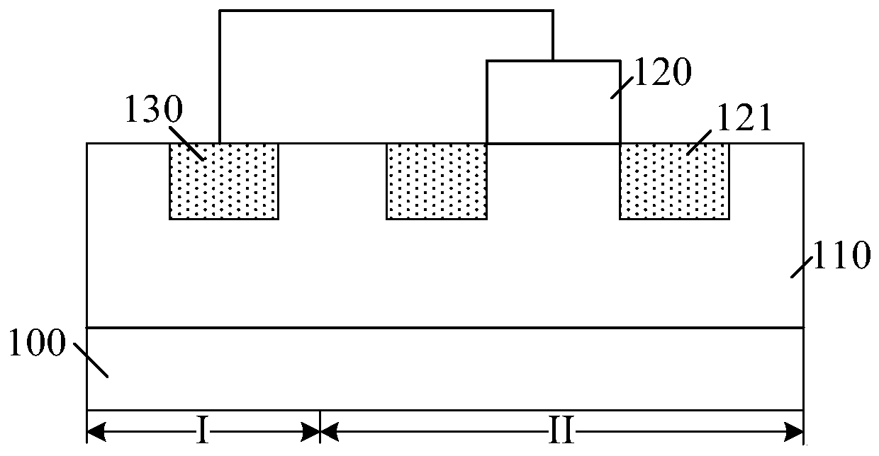
[0033] figure 1 A schematic diagram of a semiconductor structure.

[0034] Please refer to figure 1 , the semiconductor structure includes: a substrate 100, the substrate 100 includes a protection region I and a device region II; a well region 110 located in the protection region I and a device region II substrate 100; a well region located in the device region II A gate dielectric layer (not shown) on the well region 110; a gate electrode 120 located on the gate dielectric layer; a source-drain doped region 121 located in the device region II well region 110 on both sides of the gate electrode 120 ; The prote...


PUM


Abstract

The invention provides a semiconductor structure and a forming method thereof, wherein, the method comprises the following steps: a substrate; a first well region, a second well region, a third well region and a fourth well region located between the third well region and the first well region which are located in the substrate, the third well region and the second well region being the same in conductivity type of doped ions and the fourth well region and the third well region being opposite in conductivity type of doped ions; a device structure located on the third well region; a first dopedregion and a second doped region located in the first well region, the first doped region and the second doped region being separate, the conductivity type of the doped ions in the first doped regionand the second doped region being opposite to that of the first well region, the first doped region being electrically connected to the device structure; a third doped region located in the second well region, the third doped region being electrically connected to the second doped region. The first doped region, the first well region and the second doped region form a transistor, which can improve the performance of the semiconductor structure.

Description

technical field [0001] The invention relates to the technical field of semiconductor manufacturing, in particular to a semiconductor structure and a forming method thereof. Background technique [0002] As the integration level of semiconductor devices increases, the critical dimensions of transistors continue to shrink. With the drastic reduction in the size of transistors, the field of semiconductors places higher demands on the performance of semiconductor structures. [0003] In the process of forming semiconductor structures, the application of plasma is more and more extensive. However, the plasma is charged and easily affects the working process of the transistor. Therefore, in order to reduce the impact of plasma on the performance of the transistor, the transistor needs to be protected by a protective structure. The protection structure is a switch device, and when the plasma accumulated on the transistor is large, the protection structure is turned on, and the c...

Claims


Application Information

Patent Timeline
Patent Type & Authority Patents(China)
IPC IPC(8): H01L23/58H01L27/02
CPCH01L23/58H01L27/0262H01L27/0296
Inventor 蒋昊金秋敏
Owner SEMICON MFG INT (SHANGHAI) CORP
Why Eureka
Try Eureka