Circuit board procesing method

A processing method and circuit board technology, which is applied in the direction of printed circuit, printed circuit, printed circuit manufacturing, etc., can solve the problems such as the difficulty in separating the reinforcement and holding board from the circuit board, so as to simplify the peeling workload, reduce the peeling area, reduce the The effect of glue amount

Active Publication Date: 2018-12-18
NINGBO SUNNY OPOTECH CO LTD
View PDF4 Cites 2 Cited by
  • Summary
  • Abstract
  • Description
  • Claims
  • Application Information

AI Technical Summary

Problems solved by technology

However, when a large amount of adhesive is applied, it will be difficult to separate the reinforcement and holding board from the circuit board

Method used


Image

  • Circuit board procesing method
  • Circuit board procesing method
  • Circuit board procesing method

Examples


Embodiment Construction

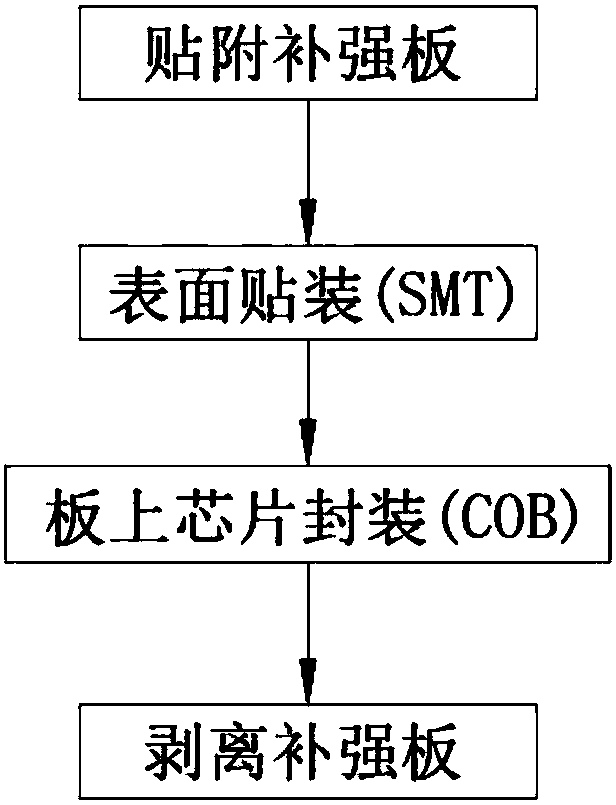
[0025] figure 1 It is a flowchart schematically showing the circuit board processing method according to the present invention. As shown in the figure, according to the circuit board processing method of the present invention, the specific steps are as follows:

[0026] a) Glue the reinforcement board 2 on the first surface 11 of the circuit board 1. The area of ​​the reinforcement board 2 is at least 85% of the area of ​​the first surface 11 of the circuit board 1. At 80-170°C, the first surface The peel strength between 11 and the reinforcing plate 2 is greater than 35.0gf / mm;

[0027] b) surface mount (SMT) on the second surface 12 of the circuit board 1;

[0028] c) performing chip-on-board packaging (COB) on the second surface 12 of the circuit board 1;

[0029] d) Peel off the reinforcement board 2 from the first surface 11 of the circuit board 1 .

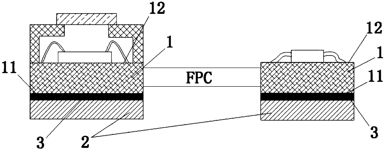
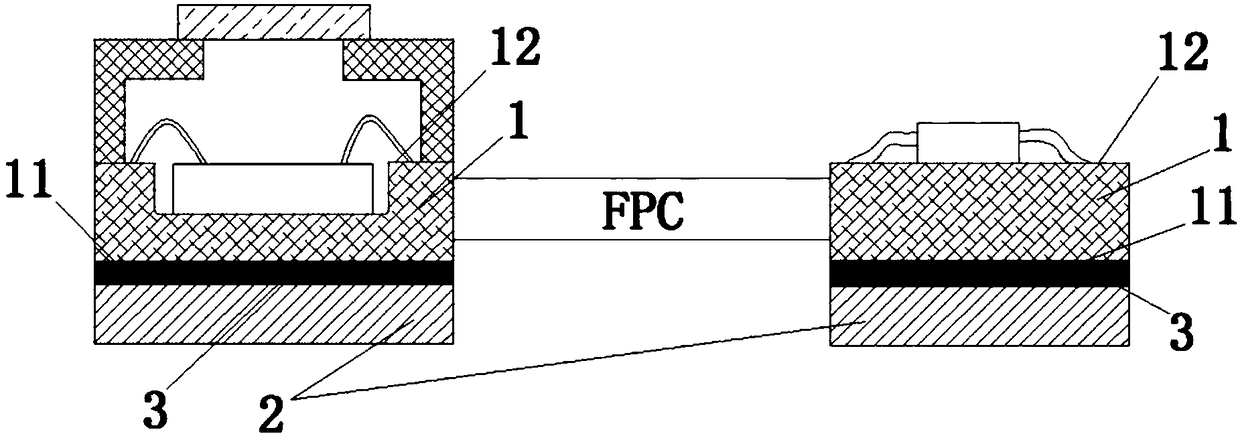
[0030] figure 2 It is a schematic diagram of an embodiment of the circuit board processing method according to the p...


PUM


Abstract

The invention relates to a circuit board processing method, comprising: a) bonding a reinforcing plate on a first surface of the circuit board, wherein the area of the reinforcing plate is at least 85% of the area of the first surface of the circuit board, and in the range of 80 to 170 DEG C, the peeling strength between the first surface and the reinforcement plate is greater than 35.0 gf / mm; b)performing surface mounting (SMT) on the second surface of the circuit board; c) performing chip-on-board (COB) packaging on the second surface of the circuit board; and d) peeling the reinforcementplate from the first surface of the circuit board. According to the method of the invention, the deformation of the circuit board in the processing process can be effectively controlled. By effectively controlling the area ratio of the reinforcing board to the circuit board to be processed, the deformation of the circuit board can be avoided in the reflow soldering process, the area of the reinforcing board can be reduced, and the peeling workload and the peeling difficulty of the reinforcing board can be simplified and reduced.

Description

technical field [0001] The invention relates to the field of printed circuit boards, in particular to a circuit board processing method. Background technique [0002] At present, with the advancement of science and technology, the update speed of electronic equipment products is getting faster and faster. Take the mobile phone industry as an example. With the continuous upgrading of mobile phones, "ultra-thin" mobile phones are becoming more and more popular. Moreover, the camera function of modern mobile phones is already essential, but due to the complex structure of the mobile phone lens module, the thickness of the mobile phone is also limited by the mobile phone lens. In the lens module, the thickness of the circuit board directly affects the height of the lens module, but the thinner the circuit board, the easier it is to deform during processing. [0003] In order to avoid deformation of the circuit board during processing, a reinforcement holding plate is usually a...

Claims


Application Information

Patent Timeline
Patent Type & Authority Applications(China)
IPC IPC(8): H05K3/22H05K3/34
CPCH05K3/22H05K3/341H05K2201/2009
Inventor 易峰亮郭巍王雅菲
Owner NINGBO SUNNY OPOTECH CO LTD
Why Eureka
Try Eureka