Back-illuminated CMOS image sensor and forming method thereof

An image sensor, back-illuminated technology, applied in the direction of electric solid-state devices, semiconductor devices, electrical components, etc., can solve the problems of reducing the charge collection volume and quantum efficiency of photodiodes, and achieve the effect of increasing the full well capacity

Inactive Publication Date: 2018-12-21
SHANGHAI HUALI MICROELECTRONICS CORP
View PDF5 Cites 6 Cited by
  • Summary
  • Abstract
  • Description
  • Claims
  • Application Information

AI Technical Summary

Problems solved by technology

However, as the pixel area continues to decrease, the volume and quantum efficiency of photodiode charge collection are undesirably reduced.

Method used


Image

  • Back-illuminated CMOS image sensor and forming method thereof
  • Back-illuminated CMOS image sensor and forming method thereof

Examples


Embodiment Construction

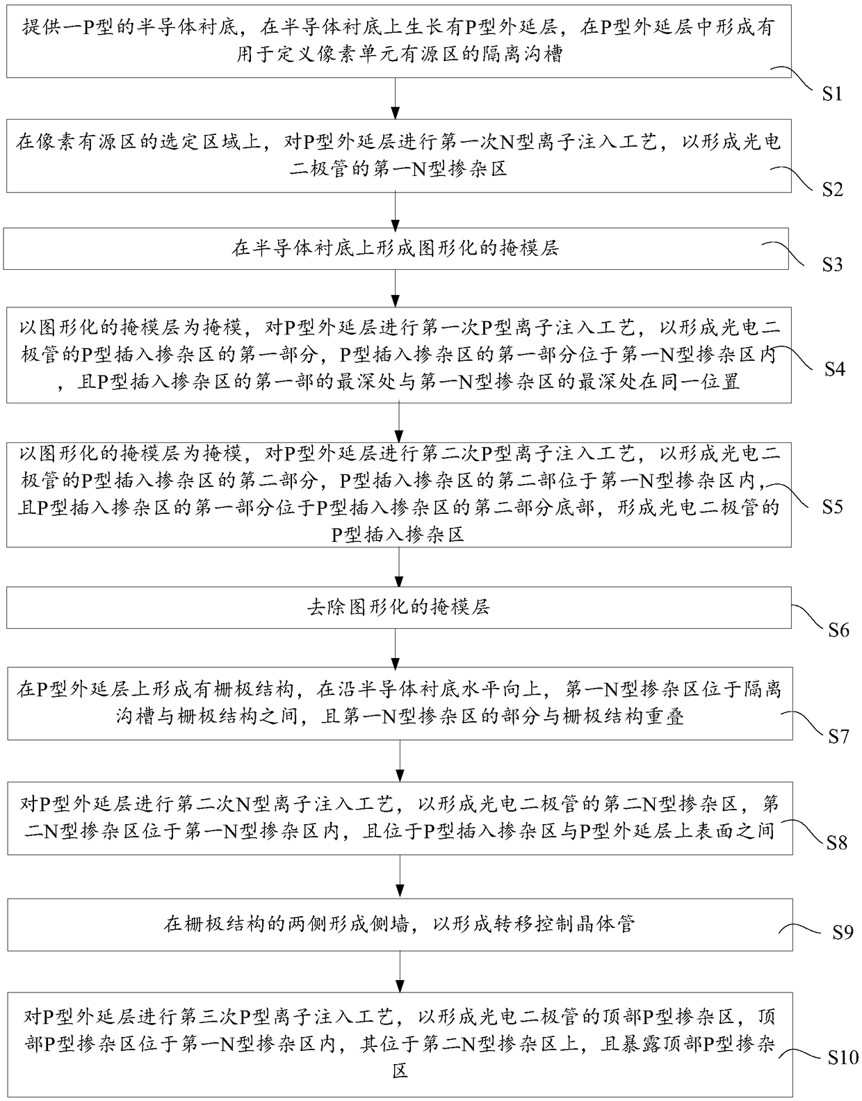
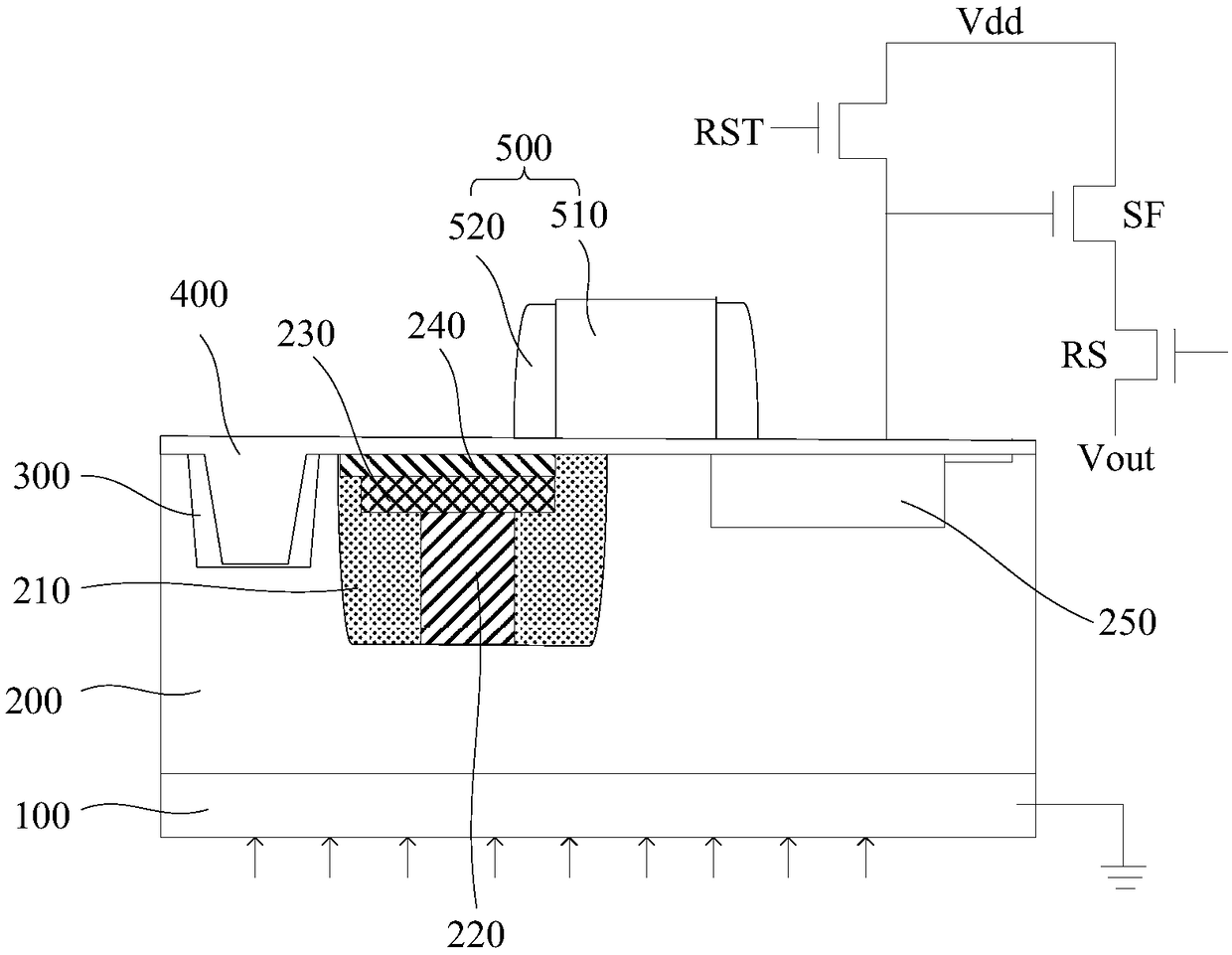
[0025] As described in the background technology, with the continuous reduction of pixel size, the pixel area is also reduced, so that the maximum signal charge that can be accommodated in the charge collection potential well of a photodiode (Photo-Diode, referred to as PD) is the full well capacity (abbreviation, well capacity) is suppressed, and the suppression of the well capacity will deteriorate the dynamic range, signal-to-noise ratio and sensitivity of small-sized pixels, and these indexes will directly affect the imaging quality of small-sized pixels.

[0026] The inventors have found that when the pixel size decreases, the junction depth of the PN junction of the photodiode becomes shallower, and this change affects the well capacity and quantum efficiency of the photodiode, thereby affecting the pixel performance of the image sensor.

[0027] Based on the above research, the present invention provides a back-illuminated CMOS image sensor and its forming method, by per...


PUM


Abstract

The invention provides a back-illuminated CMOS image sensor and a forming method thereof. The forming method of the back-illuminated CIS comprises the following steps: a P-type epitaxial layer is grown on a semiconductor substrate; an isolation trench for defining an active region of a pixel unit is formed in the P-type epitaxial layer; Forming a first N-type doped region of the photodiode on a selected region of the pixel active region; The first P-type ion implantation process is carried out on the P-type epitaxial layer by using the patterned mask layer as a mask to form a first part of theP-type insertion doped region of the photodiode, and the first part of the P-type insertion doped region is located in the first N-type doped region; A second P-type ion implantation process is carried out on the P-type epitaxial layer so as to form a second portion of the P-type insertion doped region of the photodiode, the second portion of the P-type insertion doped region being located in thefirst N-type doped region to deepen the junction depth of the PN junction of the photodiode, thereby facilitating the charge depletion of the first N-type doped region, thereby improving the full well capacity of the back-illuminated CMOS image sensor.

Description

technical field [0001] The invention relates to the field of integrated circuit manufacturing, in particular to a back-illuminated CMOS image sensor and a forming method thereof. Background technique [0002] CMOS image sensor (CIS) product is a semiconductor device for image collection and processing. Photodiode (Photo-Diode, referred to as PD) is used in CIS products as a photoelectric conversion device, so that CIS products can convert optical signals into electrical signals for storage. and display. Existing CIS products have adopted the back-illuminated (Back-illuminated) process, that is, after the semiconductor substrate is completed with MOS transistors and metal wiring, the back of the semiconductor substrate will be ground (the purpose is to reduce the thickness of the semiconductor substrate ), let the back of the semiconductor substrate serve as a light-sensing window, and the front of the semiconductor substrate will be bonded to other auxiliary semiconductor s...

Claims


Application Information

Patent Timeline
Patent Type & Authority Applications(China)
IPC IPC(8): H01L27/146
CPCH01L27/1464H01L27/14683
Inventor 庞浩秋沉沉
Owner SHANGHAI HUALI MICROELECTRONICS CORP
Why Eureka
Try Eureka