Fabrication method, system and display substrate for OLED luminescent layer thin film
A production method and production system technology, applied in the field of display devices, can solve the problems of device life and display effects, poor film morphology, poor uniformity, etc., and achieve the effects of weakening the coffee ring phenomenon, balancing drying speed, and improving uniformity
- Summary
- Abstract
- Description
- Claims
- Application Information
AI Technical Summary
Problems solved by technology
Method used
Image

Examples
preparation example Construction
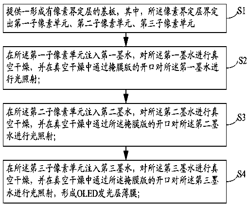
[0056] In the process of film preparation, in order to avoid the phenomenon that the boundary of the film formed after the ink is leveled on the substrate is uneven or exceeds the range of the substrate, a barrier (Bank) is usually set at the boundary of the ink printing on the substrate. In order to simplify the manufacturing process, the barrier wall and the pixel definition layer (PDL) are formed by one mask and exposure.
[0057] Step S2 , injecting the first ink into the first sub-pixel unit, vacuum drying the first ink, and irradiating the first ink with light through the opening of the mask plate during the vacuum drying.
[0058] Wherein, the step S2 specifically includes:
[0059] Step S21, injecting the first ink into the first pixel unit;
[0060] Step S22, making a one-to-one correspondence between the openings of the mask and the first sub-pixel units;
[0061] Step S23, vacuum drying the first ink, and irradiating the first ink with infrared light through the o...
Embodiment 1
[0086] Based on Embodiment 1 of the present invention, Embodiment 2 of the present invention provides a manufacturing system for OLED light-emitting layer films, including: an ink injection device, a drying chamber, a light source and a mask disposed in the drying chamber, wherein,
[0087] The ink injection device is used to inject the first ink, the second ink, and the second sub-pixel into the first sub-pixel unit, the second sub-pixel unit, and the third sub-pixel unit defined by the pixel-defining layer on a substrate formed with a pixel-defining layer. the second ink and the third ink;
[0088] a drying chamber for vacuum drying the first ink, the second ink and the third ink;
[0089] a light source, located above the mask plate, for providing illumination light;
[0090] Wherein, during the vacuum drying process of the first ink, the second ink, and the third ink in the drying chamber, the first ink, the second ink, and the third ink are dried through the opening of t...
Embodiment 2
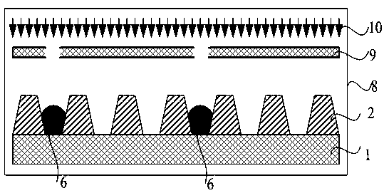
[0094] Based on Embodiment 2 of the present invention, Embodiment 3 of the present invention provides a display substrate. The display substrate includes: a glass substrate, and a pixel defining layer formed on the glass substrate; formed film.
[0095] Specifically, when the display substrate is an OLED display substrate, the thin film is an organic layer, and when the display substrate is a liquid crystal display substrate, the thin film is a color filter layer.
[0096] The following combination Figure 4 The manufacturing method of the OLED light-emitting layer thin film of the present invention will be described in detail.
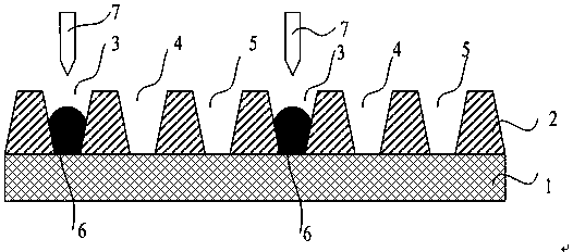
[0097] A glass substrate 1 is provided, and a pixel defining layer and a blocking wall 2 are formed on the glass substrate 1, and the blocking wall 2 and the pixel defining layer (PDL) are formed by one mask and exposure. The pixel defining layer defines a plurality of first sub-pixel units 3 , second sub-pixel units 4 and third sub-pixel units 5 . ...
PUM
 Abstract
Description
Claims
Application Information