Reaction chamber and semiconductor processing equipment

A reaction chamber and cavity technology, which is applied in semiconductor/solid-state device manufacturing, discharge tubes, electrical components, etc., can solve problems such as affecting process efficiency, high equipment cost, and the lack of process adjustment capabilities of process sleeves. Process efficiency, reduced equipment costs, increased flexibility

Active Publication Date: 2018-12-25
BEIJING NAURA MICROELECTRONICS EQUIP CO LTD
View PDF7 Cites 4 Cited by
  • Summary
  • Abstract
  • Description
  • Claims
  • Application Information

AI Technical Summary

Problems solved by technology

[0004] However, the size of the above-mentioned process sleeve is fixed, which makes it necessary to design process sleeves of different sizes for wafers with different diameters, resulting in higher equipment costs, and when processing wafers with different diameters in the same react

Method used


Image

  • Reaction chamber and semiconductor processing equipment
  • Reaction chamber and semiconductor processing equipment
  • Reaction chamber and semiconductor processing equipment

Examples


Example Embodiment

[0032] In order for those skilled in the art to better understand the technical solution of the present invention, the reaction chamber and semiconductor processing equipment provided by the present invention will be described in detail below in conjunction with the accompanying drawings.
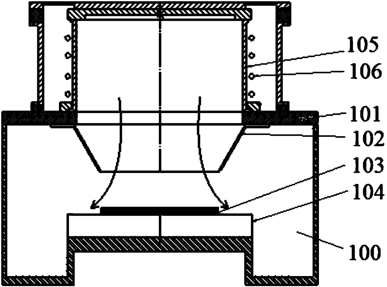
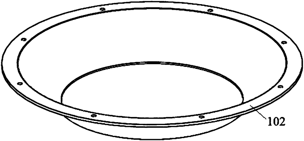
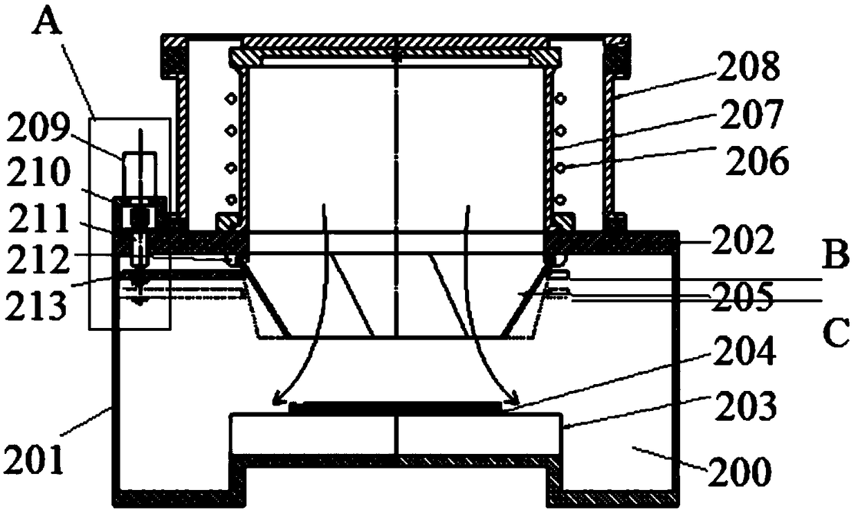
[0033] Please also refer to image 3 and Figure 4 , the reaction chamber 200 provided in this embodiment includes a cavity 201 and a plasma source, wherein a base 203 for carrying a workpiece 204 to be processed is arranged in the cavity 201, and on the top wall 202 of the cavity 201 A top wall opening is provided, and a plasma source is provided above the top wall opening. The plasma source is used to generate plasma, and the plasma diffuses downwards into the cavity 201 through the top wall opening. Specifically, the plasma source includes a dielectric cylinder 207 and a radio frequency coil 206 surrounding the dielectric cylinder 207. By applying radio frequency power to the radio freq...


PUM


Abstract

The invention provides a reaction chamber and semiconductor processing equipment. The reaction chamber includes a cavity. A pedestal used for bearing a to-be-processed workpiece is arranged in the cavity. A process sleeve is arranged above the pedestal. Plasma diffuses to the surface of the to-be-processed workpiece through the process sleeve. Furthermore, the process sleeve includes multiple sub-baffles. The multiple sub-baffles are arranged in order to form a ring. The upper ends of the sub-baffles are rotatably connected to the cavity. The size of a lower opening of the ring is adjusted bychanging inclination angles of the sub-baffles relative to the vertical direction. The reaction chamber provided by the invention can improve the process efficiency, reduce the equipment cost, and improve the flexibility of process result optimization.

Description

technical field [0001] The invention relates to the technical field of semiconductor manufacturing, in particular to a reaction chamber and semiconductor processing equipment. Background technique [0002] In recent years, with the continuous expansion and application of micro-electromechanical device systems in the field of consumer electronics, and the broad prospects of TSV (Throughout Silicon Vias) through-hole etching technology in the future packaging field, the dry plasma deep silicon etching process has gradually become One of the mainstream processes in the field of micro-electromechanical processing and TSV technology, it has a plasma source that generates high-energy plasma, and bombards the wafer under the guidance of the lower bias system, thereby producing a series of physical and chemical effects on the wafer surface. [0003] figure 1 For a cutaway view of an existing reaction chamber, see figure 1 , the reaction chamber 100 includes a cavity, and a base 10...

Claims


Application Information

Patent Timeline
IPC IPC(8): H01J37/32H01L21/67
CPCH01J37/32807H01J2237/334H01L21/67069
Inventor 李璐
Owner BEIJING NAURA MICROELECTRONICS EQUIP CO LTD
Why Eureka
Try Eureka