Optical fingerprint identification device and preparation method thereof

A fingerprint recognition and optical technology, applied in character and pattern recognition, acquisition/organization of fingerprints/palmprints, instruments, etc., can solve the problem of high signal-to-noise ratio between fingerprint signal and light source signal, avoid light leakage interference, accuracy and use The effect of fewer conditions and improved identification ability

Active Publication Date: 2019-01-04
GUAN YEOLIGHT TECH CO LTD
View PDF11 Cites 13 Cited by
  • Summary
  • Abstract
  • Description
  • Claims
  • Application Information

AI Technical Summary

Problems solved by technology

[0006] Therefore, the technical problem to be solved by the present invention is to overcome the problem that the signal-to-noise ratio between the fingerprint signal and the light source signal in the planar light source in the prior art is too high, thereby providing an optical fingerprint identification device and its preparation method

Method used


Image

  • Optical fingerprint identification device and preparation method thereof
  • Optical fingerprint identification device and preparation method thereof
  • Optical fingerprint identification device and preparation method thereof

Examples


Embodiment 1

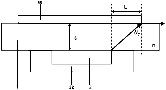
[0043] In order to prevent some light from directly entering the transparent substrate, refracting it out, and then encountering the finger and reflecting it into the optical sensor 4, the present invention preferably sets a first light-shielding layer on the transparent substrate 1 around the finger touch area 11. 53 , the first light-shielding layer 53 is located right above the light source 2 . Some of the emitted direct light will directly enter the transparent substrate 1, and then be absorbed by the first light-shielding layer 53 covering it, so as to prevent the light that does not enter the finger touch area 11 from being directly refracted and affect the performance of the fingerprint recognition device. beautiful.

[0044] The material of the first light-shielding layer here has no special requirements, as long as it is opaque, the purpose of the invention can be achieved, and it can be a metal layer, such as Mo / Al / Mo, Ag, and the like.

[0045] Preferably, as fig...

Embodiment 2

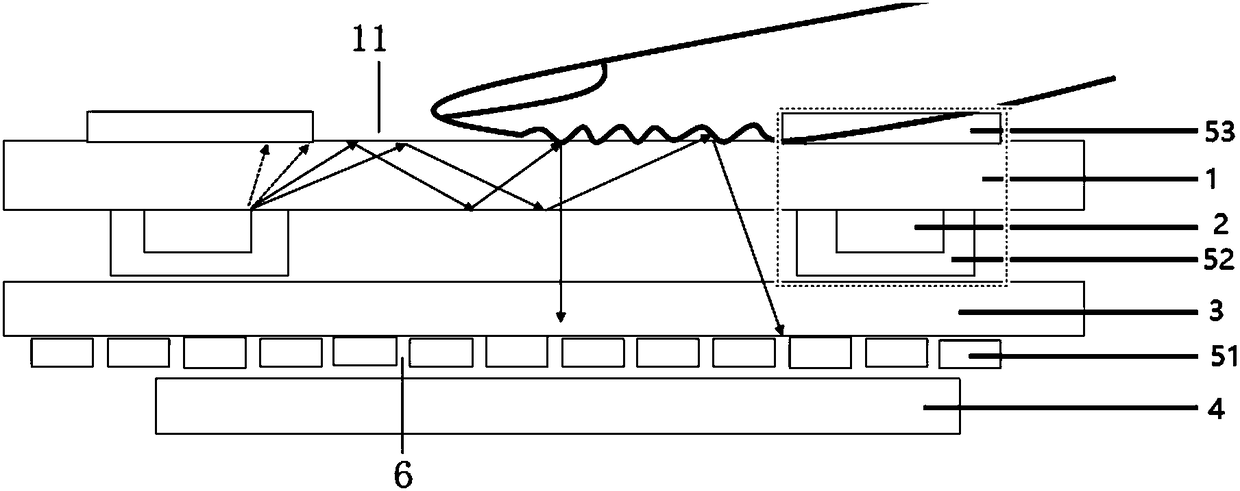
[0050] Such as figure 1 As shown, in order to further reduce the noise of the fingerprint optical recognition device, an encapsulation layer 3 and a second light-shielding layer 51 are also provided between the finger touch area 11 and the optical sensor 4. A light hole 6 is arranged directly above the optical sensor 4 .

[0051] The opaque light source seat 52 in this embodiment is disposed on the transparent encapsulation layer 3 , and the second light-shielding layer 51 is disposed on the outer surface of the encapsulation layer 3 .

[0052] The present invention has no special requirements on the material of the second light-shielding layer 51 , as long as it is opaque, the purpose of the invention can be achieved, and it can be a metal layer, such as Mo / Al / Mo, Ag, etc.

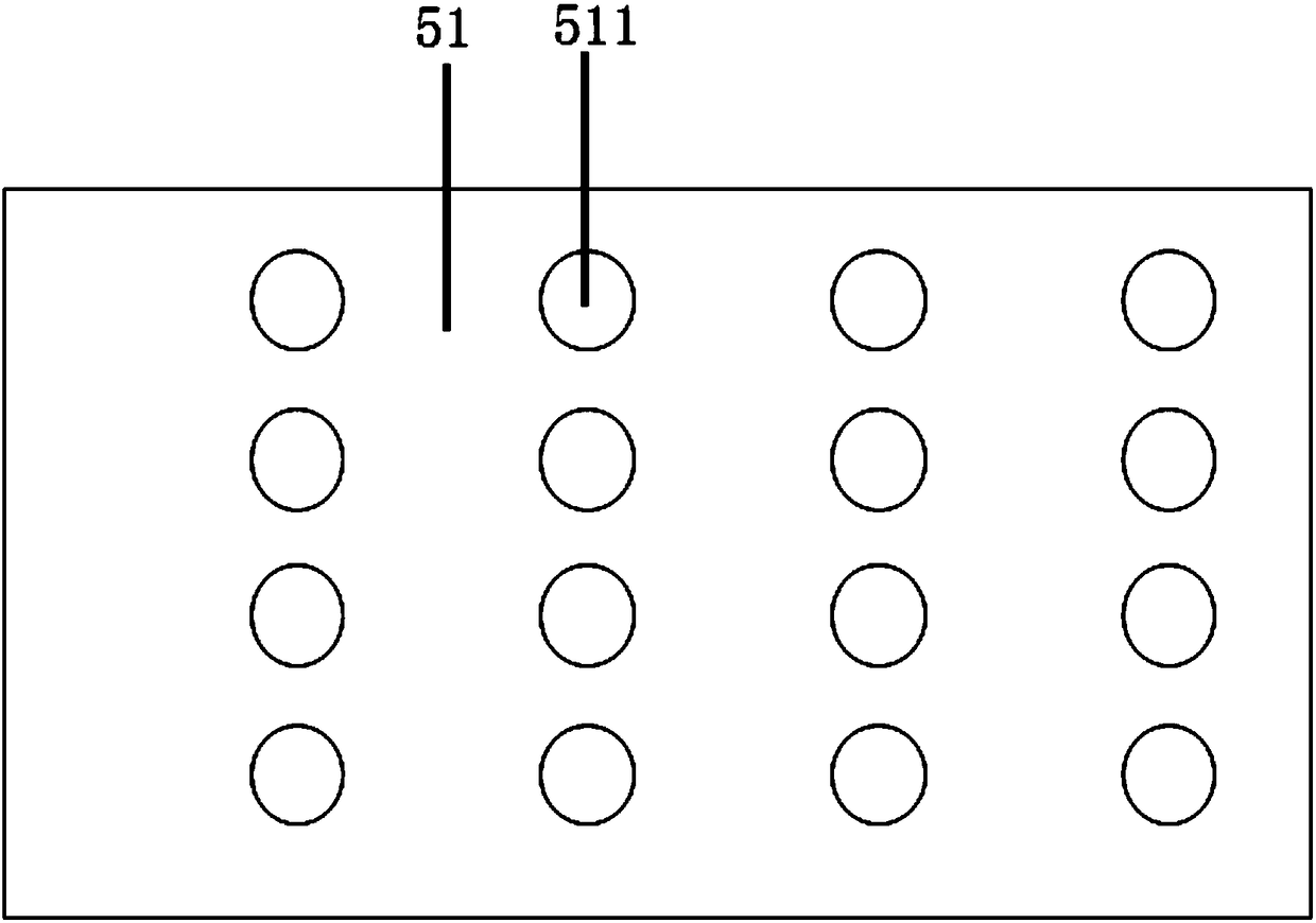
[0053] The diameter of the clear hole is 10um-500um, preferably 15um in the present invention, and the distance between adjacent clear holes is 10um-10mm, preferably 0.68mm in the present invention, such...

Embodiment 3

[0058] The difference from Example 2 is that, as Figure 4 As shown, the opaque light source seat 52 is disposed on the second light-shielding layer 51 , and the second light-shielding layer 51 is disposed on the inner side of the encapsulation layer 3 .

[0059] When a finger is pressed on the finger touch area 11, the light reflected by the transparent substrate 1 is filtered by the second light-shielding layer 51 before reaching the optical sensor 4, and the light after passing through the light hole 6 passes through the encapsulation layer After 3, it is finally captured by the optical sensor 4, and part of the light that does not enter the light hole 6 will be blocked or absorbed by the second light-shielding layer 51. Using the principle of small hole imaging, high-definition fingerprint graphics can be obtained. It is beneficial to improve the recognition accuracy of the optical sensor to the fingerprint image.

[0060] Such as Figure 4 As shown, the method for speci...


PUM


Abstract

The invention discloses an optical fingerprint identification device and a preparation method thereof, comprising a transparent substrate, a luminescent light source and an optical inductor. The luminescent light source is located in all or part of the peripheral area of the finger contact pressure area and is located below the transparent substrate. The optical sensor is arranged below the fingertouch pressure area, and the luminous light source is a planar light source. The luminous light source is also provided with a light shielding structure for limiting the light emitting angle of the light source. The light emitted from the luminous light source enters the finger touch pressure area after being shielded by the light shielding structure. An optical fingerprint identification apparatus The planar light source can effectively reduce the thickness of the device, meanwhile, a light-shielding structure is arranged on the planar light source, part of the light emitted from the planarlight source can be blocked by the light-shielding structure, thereby avoiding the light leakage interference of some light rays, greatly reducing the signal-to-noise ratio of the fingerprint signal and the light source signal device, and improving the identification ability of the fingerprint signal.

Description

technical field [0001] The invention relates to the technical field of optical fingerprint identification, in particular to an optical fingerprint identification device and a preparation method thereof. Background technique [0002] The optical fingerprint collector is an optical fingerprint collector that requires its own light source. The current light source uses LED chips and light guide plates, which have the disadvantages of low energy efficiency, uneven illumination, high assembly requirements, and high cost. [0003] The current mainstream technologies of fingerprint identification technology are capacitive fingerprint identification technology and optical fingerprint identification technology; capacitive type currently has the advantage of small size and is widely used in mobile devices, such as: mobile phones, notebooks, tablet computers, etc. The above requirements are relatively strict. The reason is that the sensor is used to identify the "capacitance" signal. B...

Claims


Application Information

Patent Timeline
Patent Type & Authority Applications(China)
IPC IPC(8): G06K9/00
CPCG06V40/1341G06V40/1318
Inventor 李育豪李栋栋朱映光谢静胡永岚
Owner GUAN YEOLIGHT TECH CO LTD
Why Eureka
Try Eureka