Device and method for testing high-temperature electrical characteristics of semiconductor devices

A test method and test device technology, which are applied in the direction of single semiconductor device testing, measuring devices, instruments, etc., can solve the problem of inability to quickly and accurately realize the high-temperature electrical characteristics test of semiconductor devices, and achieve easy automatic testing and continuous large-scale batches. The effect of testing, testing process safety

Active Publication Date: 2021-01-01
GLOBAL ENERGY INTERCONNECTION RES INST CO LTD
View PDF10 Cites 0 Cited by
  • Summary
  • Abstract
  • Description
  • Claims
  • Application Information

AI Technical Summary

Problems solved by technology

[0004] Therefore, the present invention provides a method and device for testing the high-temperature electrical characteristics of semiconductor devices, which overcomes the defects in the prior art that the high-temperature electrical characteristics of semiconductor devices cannot be tested quickly and accurately.

Method used


Image

  • Device and method for testing high-temperature electrical characteristics of semiconductor devices
  • Device and method for testing high-temperature electrical characteristics of semiconductor devices
  • Device and method for testing high-temperature electrical characteristics of semiconductor devices

Examples


Embodiment 1

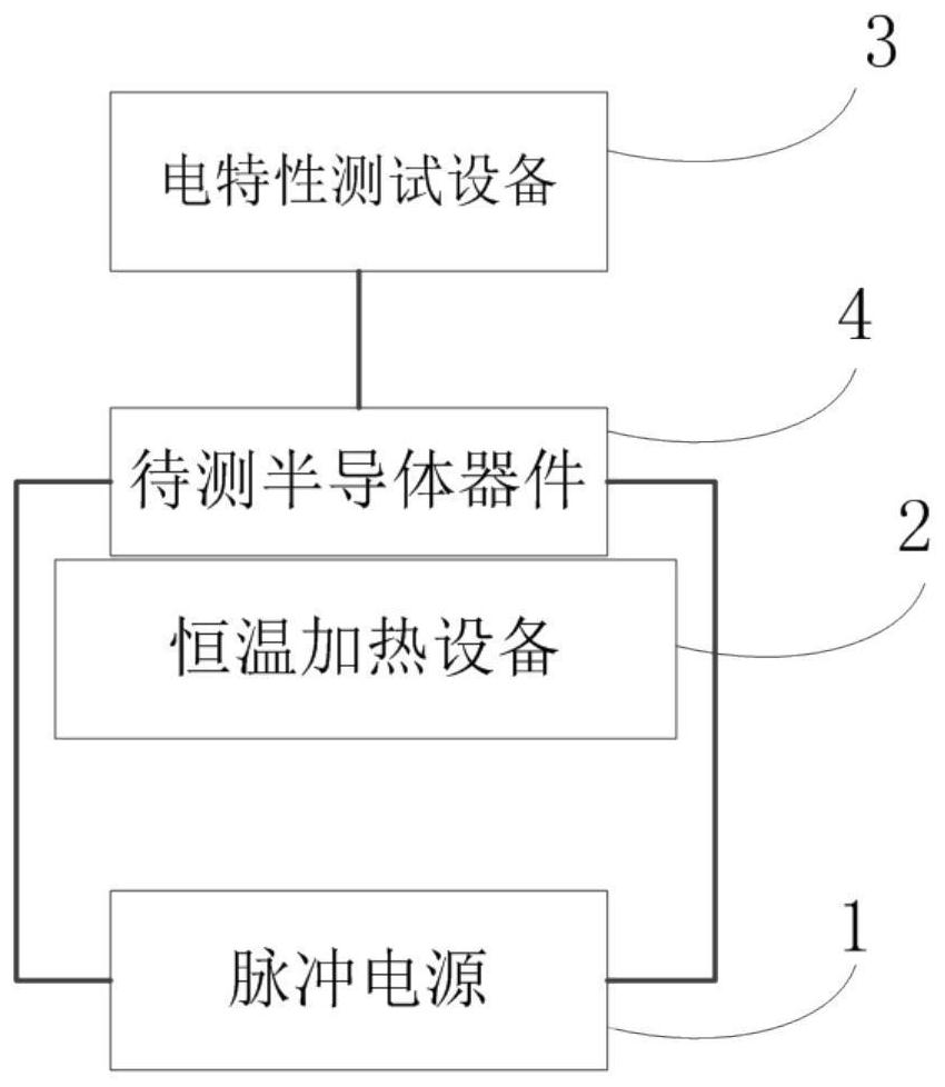
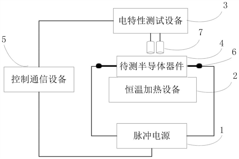
[0032] An embodiment of the present invention provides a semiconductor device high temperature electrical characteristic testing device, such as figure 1 As shown, it includes: pulse power supply 1, constant temperature heating equipment 2, and electrical characteristic testing equipment 3.

[0033] To conduct high-temperature electrical characteristic tests on semiconductor devices, they need to be heated first. In the embodiment of the present invention, within the first preset time, the pulse power supply 1 provides current pulses to the semiconductor device 4 to be tested, and the constant temperature heating device 2 heats the semiconductor device 4 to be tested.

[0034] In the embodiment of the present invention, the semiconductor device to be tested has a turn-on voltage drop when current flows, and the current pulse can be a current pulse signal with a preset current value and a preset duration determined according to a preset target temperature. Such as Figure 4 A...

Embodiment 2

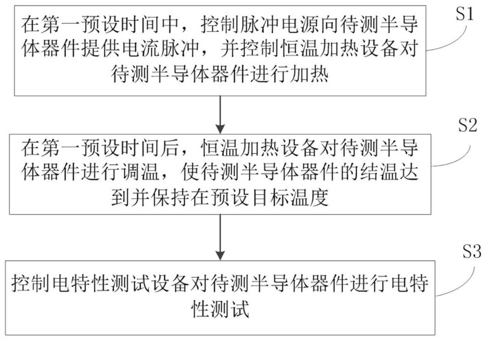
[0046] An embodiment of the present invention provides a method for testing the high-temperature electrical characteristics of a semiconductor device, such as image 3 shown, including the following steps:

[0047] Step S1: During the first preset time, control the pulse power supply to provide current pulses to the semiconductor device to be tested, and control the constant temperature heating device to heat the semiconductor device to be tested. In the embodiment of the present invention, the semiconductor device to be tested has a turn-on voltage drop when current flows, and the current pulse can be a current pulse signal with a preset current value and a preset duration determined according to a preset target temperature.

[0048] Such as Figure 4 As shown, in the embodiment of the present invention, the semiconductor device to be tested is heated to a temperature close to the test target temperature T after the preset current heating time t1 j-set , such as the target ...


PUM


Abstract

The invention discloses a high-temperature electrical characteristic testing device and a method for a semiconductor device. The device comprises a pulse power supply, a constant temperature heating equipment, and an electrical characteristic testing equipment. The method comprises the following steps of during a first preset time, the pulse power supply supplies a current pulse to a device to betested, and the constant temperature heating equipment heats the device to be tested; after the first preset time, the connection between the pulse power source and the device to be tested is disconnected, the constant temperature heating equipment adjusts the temperature of the device to be tested, so that the junction temperature of the device to be tested reaches and maintains the target temperature; the electrical characteristic testing equipment performs a high-temperature electrical characteristic test on the device to be tested. By implementing the high-temperature electrical characteristic testing device and method for semiconductor device, the device to be tested is heated by the combination of its own loss and the constant temperature heating device, the heating rate is fast; theelectrical characteristic testing equipment is not in contact with the device during the temperature rise of the device to avoid being affected by high temperature; the pulse power supply and the electrical characteristic testing equipment are disconnected during the test so as to prevent the two devices from interacting with each other, the testing process is safer and can be quickly and extensively tested in large batches.

Description

technical field [0001] The invention relates to the technical field of testing high-temperature electrical characteristics of semiconductor devices, in particular to a device and method for testing high-temperature electrical characteristics of semiconductor devices. Background technique [0002] Semiconductor devices based on semiconductor materials will generate certain losses while realizing specific functions. These losses are usually expressed in the form of heat, which will increase the temperature of the device itself and the environment. The electrical characteristics of semiconductor devices often change due to changes in temperature. Therefore, semiconductor devices usually need to be tested for their electrical characteristics at high temperatures before they are manufactured or used, so as to screen out samples with unqualified parameters. In addition, the electrical characteristics test of semiconductor devices under high temperature conditions can also expose ...

Claims


Application Information

Patent Timeline
Patent Type & Authority Patents(China)
IPC IPC(8): G01R31/26
CPCG01R31/2601
Inventor 查祎英金锐李玲董少华吴鹏飞张璧君杨霏潘艳
Owner GLOBAL ENERGY INTERCONNECTION RES INST CO LTD
Why Eureka
Try Eureka