A semiconductor device having an electrostatic discharge protection structure and a layout structure thereof

A protection structure and electrostatic discharge technology, applied in semiconductor devices, electric solid devices, circuits, etc., can solve problems such as no protection, low trigger voltage, MOSFET failure, etc.

Inactive Publication Date: 2019-01-15
CSMC TECH FAB2 CO LTD
View PDF3 Cites 4 Cited by
  • Summary
  • Abstract
  • Description
  • Claims
  • Application Information

AI Technical Summary

Problems solved by technology

However, when the internal circuit uses a small-width MOSFET (Metal Oxide Semiconductor Field Effect Transistor) as the port circuit, since the gate of the small-width MOSFET is in a floating state and the trigger voltage is l...

Method used


Image

  • A semiconductor device having an electrostatic discharge protection structure and a layout structure thereof
  • A semiconductor device having an electrostatic discharge protection structure and a layout structure thereof
  • A semiconductor device having an electrostatic discharge protection structure and a layout structure thereof

Examples


Embodiment Construction

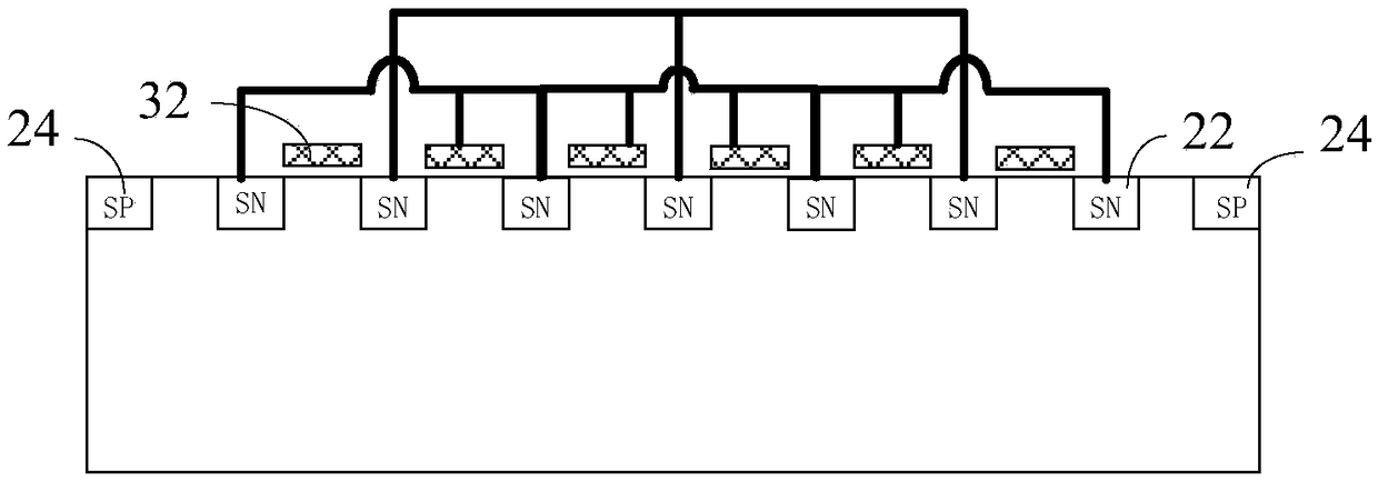
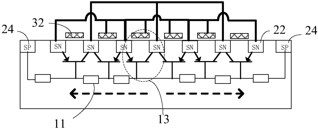
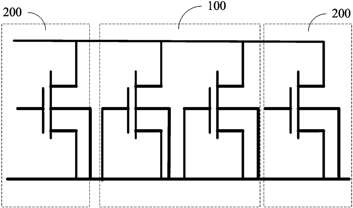
[0022] In order to facilitate the understanding of the present invention, the present invention will be described more fully below with reference to the associated drawings. A preferred embodiment of the invention is shown in the drawings. However, the present invention can be embodied in many different forms and is not limited to the embodiments described herein. Rather, these embodiments are provided so that the disclosure of the present invention will be thorough and complete.

[0023] Unless otherwise defined, all technical and scientific terms used herein have the same meaning as commonly understood by one of ordinary skill in the technical field of the invention. The terms used herein in the description of the present invention are for the purpose of describing specific embodiments only, and are not intended to limit the present invention. As used herein, the term "and / or" includes any and all combinations of one or more of the associated listed items.

[0024] The se...


PUM


Abstract

The invention relates to a semiconductor device with an electrostatic discharge protection structure and a layout structure thereof, the device includes an internal circuit and a GGNMOS, the internalcircuit includes a MOSFET, the semiconductor device further includes an active region, A MOSFET is arrange in that active region, characterized by, GGNMOS is also arrange in that active region, and the MOSFET is arranged on both lateral sides of the GGNMOS in the same active region, The active region comprises a P well, an N-type doped region of the GGNMOS and an N-type doped region of the MOSFETare arranged in the P well, the semiconductor device further comprises a P-type doped region as a substrate, and the P-type doped region is arranged on the outer sides of the MOSFET on both sides. When the electrostatic discharge occurs, if the MOSFET of the internal circuit is turned on, the substrate current is formed, thereby increasing the gate voltage of the intermediate GGNMOS, enabling theGGNMOS to be turned on more easily and improving the ESD capability.

Description

technical field [0001] The invention relates to an antistatic protection device, in particular to a semiconductor device with an electrostatic discharge protection structure. Background technique [0002] Electrostatic discharge is a common natural phenomenon in our life, but the large current generated in a short period of time during electrostatic discharge will cause fatal damage to integrated circuits, which is an important problem causing failure in the production and application of integrated circuits. [0003] A traditional electrostatic discharge (ESD) circuit protection scheme is to connect the internal circuit of the semiconductor device in parallel with GGNMOS (Gate Grounded N-channel Metal-Oxide Semiconductor Field Effect Transistor) or other ESD protection devices to protect the internal circuit. However, when the internal circuit uses a small-width MOSFET (Metal Oxide Semiconductor Field Effect Transistor) as the port circuit, since the gate of the small-width ...

Claims


Application Information

Patent Timeline
IPC IPC(8): H01L27/02
CPCH01L27/0207H01L27/0266
Inventor 汪广羊
Owner CSMC TECH FAB2 CO LTD
Why Eureka
Try Eureka