Fully isolated laterally diffused metal oxide semiconductor structure and manufacturing method

A technology of oxide semiconductors and manufacturing methods, applied in the field of LDMOS, can solve problems such as limited improvement effect, difficulty in realizing high-voltage applications, and increasing P-type substrates

Active Publication Date: 2020-04-21
CSMC TECH FAB2 CO LTD
View PDF5 Cites 0 Cited by
  • Summary
  • Abstract
  • Description
  • Claims
  • Application Information

AI Technical Summary

Problems solved by technology

The most important thing is that the thickness and concentration of the high-voltage P-type substrate (HVPWell) in the epitaxial layer are also fixed, and the P-type substrate cannot be lifted by other means so that it will not be depleted.
Therefore this limits the extension of Fully ISO NLDMOS devices to high voltage applications
[0004] One solution is to add P-type impurities at the bottom of the developed high-voltage Fully ISO NLDMOS device to increase the concentration of the P-type substrate (P-sub) and slow down the depletion of impurities; however, as an isolation terminal, the N-type buried layer ( The concentration of BN) will be very high; in addition, increasing the P-type substrate (P-sub) concentration will significantly reduce the junction breakdown voltage of the bottom P-type substrate (P-sub) and N-type buried layer (BN), It has become another constraint for the expansion of devices to high-voltage applications, so there is limited room for increasing the concentration at the bottom of the P-type substrate, and the improvement effect is also limited. High-voltage applications of 40-60V are difficult to achieve

Method used


Image

  • Fully isolated laterally diffused metal oxide semiconductor structure and manufacturing method
  • Fully isolated laterally diffused metal oxide semiconductor structure and manufacturing method
  • Fully isolated laterally diffused metal oxide semiconductor structure and manufacturing method

Examples


Embodiment Construction

[0031] In order to make the object, technical solution and advantages of the present invention clearer, the present invention will be further described in detail below in conjunction with the accompanying drawings and embodiments. It should be understood that the specific embodiments described here are only used to explain the present invention, not to limit the present invention.

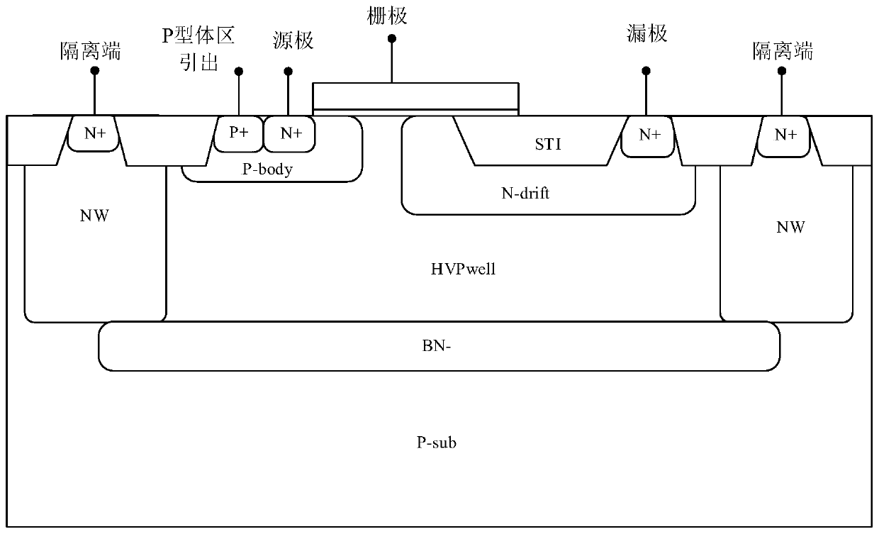
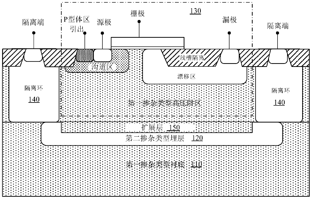
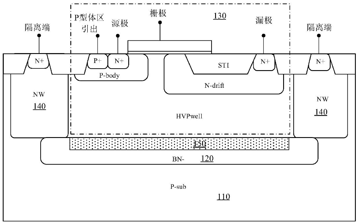
[0032] figure 2 It is a fully isolated laterally diffused metal-oxide-semiconductor structure in an embodiment. The semiconductor structure includes a substrate 110 of a first doping type, a buried layer 120 of a second doping type placed in the substrate 110 of the first doping type, and a buried layer 120 of the second doping type formed on the buried layer 120 of the second doping type. The main structure 130 in the epitaxial layer and the isolation ring 140 arranged around the main structure 130 . The buried layer 120 of the second doping type and the isolation ring 140 isolate the main stru...


PUM


Abstract

A fully-isolated laterally-diffused metal oxide semiconductor structure. The semiconductor structure comprises a substrate (110) of a first doping type, a buried layer (120) of a second doping type disposed within the substrate (110) of the first doping type, a main structure (130) formed on the buried layer (120) of the second doping type, and an isolation ring (140) disposed around the main structure (130). The buried layer (120) and the isolation ring (140) together isolate the main structure (130). The buried layer (120) of the second doping type is internally formed with an expansion layer (150) of the first doping type, and the expansion layer (150) is near to a side of the main structure (130), and is integrated with a well region within the main structure (130). Further disclosed is a manufacturing method for manufacturing the semiconductor structure.

Description

technical field [0001] The invention relates to the technical field of semiconductors, in particular to a high-voltage completely isolated N-type channel LDMOS. Background technique [0002] The structure of fully isolated (Fully Isolated) N-type channel LDMOS (NLDMOS) is as follows figure 1 As shown, compared with the traditional NLDMOS, it allows differences in the voltage bias of the drain terminal (Drain) and the isolation terminal (BN-ISO), and can ensure the stability of the electrical characteristics of the device under different isolation terminal bias voltages. It is more suitable for the application operation of power integrated circuits, and the demand is increasing. However, Fully ISO NLDMOS is still in the field of low-voltage applications, and it is difficult to extend to high-voltage applications. The main reason is that the voltage bias of the isolation terminal in the high-voltage field is large, and the P-type substrate (HVPWell) of the device is complete...

Claims


Application Information

Patent Timeline
Patent Type & Authority Patents(China)
IPC IPC(8): H01L29/06H01L29/78H01L21/336
CPCH01L29/0623H01L29/66681H01L29/7816H01L29/06H01L29/78
Inventor 王琼
Owner CSMC TECH FAB2 CO LTD
Why Eureka
Try Eureka