Fabrication method of frontal emitter junction tunneling oxidation passivation battery base on single crystal PERC

A technology of tunneling oxidation and emitter junction, applied in circuits, electrical components, final product manufacturing, etc., can solve the problems of unsatisfactory battery preparation method, poor repeatability, and high equipment cost, and achieve the effect of improving battery Voc

Inactive Publication Date: 2019-01-15
SHANGHAI SHENZHOU NEW ENERGY DEV +1
View PDF0 Cites 13 Cited by
  • Summary
  • Abstract
  • Description
  • Claims
  • Application Information

AI Technical Summary

Problems solved by technology

Selective emitter junction solar cells effectively solve this pair of contradictions, but the cost of existing equipment is high, or the repeatability is poor, and the cell preparation methods are not very ideal

Method used


Image

  • Fabrication method of frontal emitter junction tunneling oxidation passivation battery base on single crystal PERC

Examples


Embodiment 1

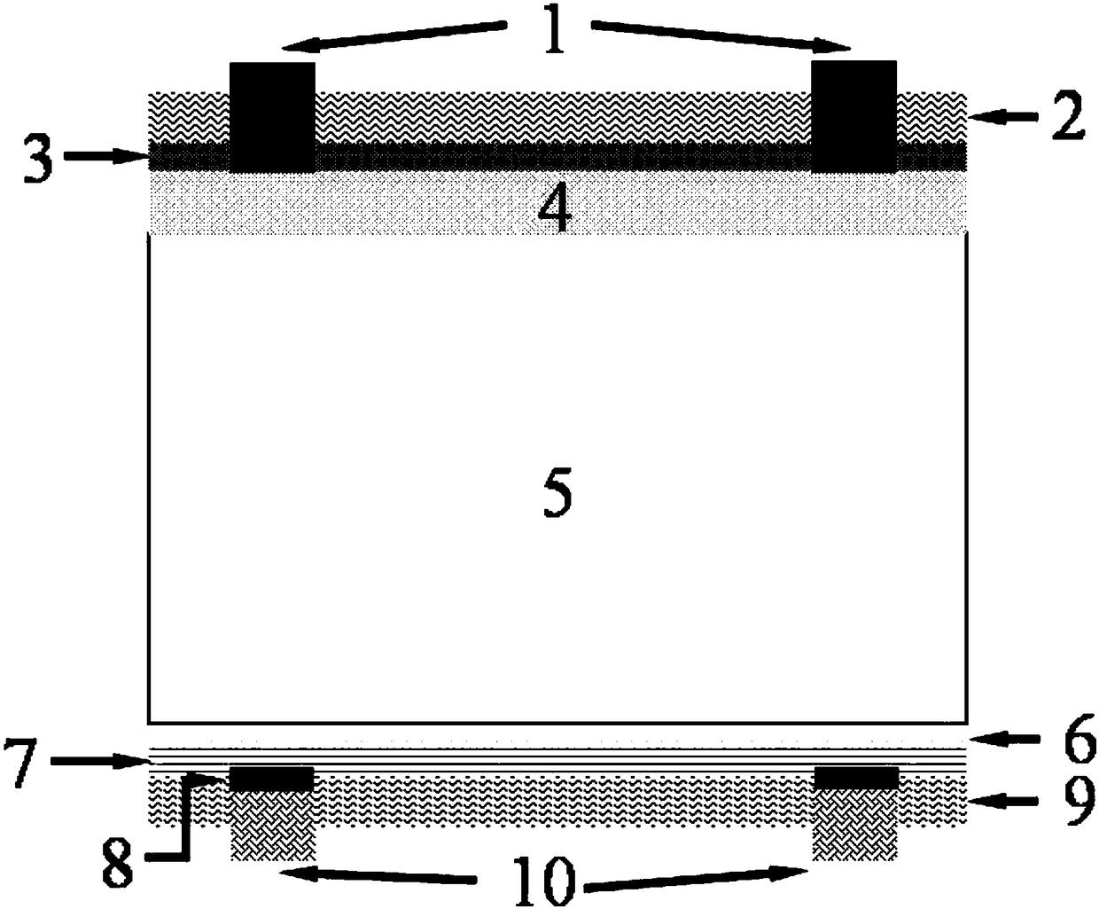
[0031] A method for preparing a front emitter junction tunneling oxidation passivation cell based on single crystal PERC technology, using the following steps:

[0032] (1) Remove the damaged layer of the silicon wafer in the alkali texturing tank and perform surface polishing and single-side texturing to form a 3 μm high pyramid textured surface;

[0033] (2) Preparation of ultra-thin tunneling oxide layer SiO on the back of the cell by wet chemical or high temperature thermal oxidation process 2 , with a thickness of 1.8-2nm, a P-doped polysilicon layer with a thickness of 50nm is deposited on the front side of the silicon wafer by CVD. The P-doped polysilicon layer is based on the PECVD method with high-purity SiH 4 The gas source is prepared and formed at 500°C-600°C, and the concentration of doped P is 5×10 20 cm -3 ;

[0034] (3) The back of the battery is selectively etched by a wet process. The wet selective etching uses a commonly used polycrystalline etching solut...

Embodiment 2

[0044] Based on the preparation method of monocrystalline PERC front emitter junction tunneling oxidation passivation cell, the following steps are adopted:

[0045] (1) Remove the damaged layer of the silicon wafer in the alkali texturing tank and perform surface polishing and single-side texturing to form a 1 μm high pyramid textured surface;

[0046] (2) Preparation of ultra-thin tunnel oxide layer SiO on the textured surface of silicon wafer 2 and P-doped polysilicon layer to form N + For the emitter junction, this embodiment uses a wet chemical process to prepare an ultra-thin tunneling oxide layer, the temperature is controlled at 50°C, the solution used is a pure nitric acid solution with a concentration of 69 wt%, and the reaction time of the silicon wafer in the solution is controlled at 50 minutes , the fabricated ultra-thin tunnel oxide SiO 2 The thickness of the doped polysilicon layer is 0.5nm, and the P-doped polysilicon layer is based on the PECVD method. The ...

Embodiment 3

[0055] Based on the preparation method of monocrystalline PERC front emitter junction tunneling oxidation passivation cell, the following steps are adopted:

[0056] (1) Remove the damaged layer of the silicon wafer in the alkali texturing tank and perform surface polishing and single-side texturing to form a 2 μm high pyramid textured surface;

[0057] (2) Preparation of ultra-thin tunnel oxide layer SiO on the textured surface of silicon wafer 2 and P-doped polysilicon layer to form N + For the emitter junction, this embodiment uses a wet chemical process to prepare an ultra-thin tunneling oxide layer, the temperature is controlled at 120°C, the solution used is a pure nitric acid solution with a concentration of 69 wt%, and the reaction time of the silicon wafer in the solution is controlled at 30 minutes , the fabricated ultra-thin tunnel oxide SiO 2 The thickness of the doped polysilicon layer is 1nm, and the P-doped polysilicon layer is based on the PECVD method. CVD e...


PUM

PropertyMeasurementUnit
thicknessaaaaaaaaaa
thicknessaaaaaaaaaa
thicknessaaaaaaaaaa

Abstract

A method for manufacture a front emitter junction tunnel oxidation passivation battery based on a single crystal PERC, comprises a single crystal silicon wafer dedamaged layer, surface polishing, single sided velvet making, A sup thin tunneling oxide lay SiO2 and a P-doped polycrystalline silicon layer are prepared on that pile surface of a silicon wafer to form an N + emit junction, the phosphorus-doped polycrystalline silicon layer on the back side is removed by wet selective etching, A high-temperature anneal process activate that phosphorus-doped polycrystalline silicon layer on the frontsurface, Al2O3 layer is deposited on the back of the battery, and hydride amorphous silicon nitride passivation antireflection layer is deposited on the front / back of the battery. The back passivationlayer is selectively patterned and opened by ns laser. Finally, the back aluminum paste / back electrode and the front metal electrode grid line are printed on the screen to form the metallized ohmic contact of the front and back electrodes. As that selective tunnel capability is adopted, the metal on the surface of the emit junction is reduced. Semiconductor surface recombination and process technology route compatible with the existing high-efficiency single crystal PERC battery fabrication process is conducive to reduce equipment investment costs.

Description

technical field [0001] The invention relates to a method for preparing a solar cell, in particular to a method for preparing a cell based on single-crystal PERC front-side emitter junction tunneling oxidation passivation. Background technique [0002] With the development of the solar photovoltaic market, people's demand for high-efficiency crystalline silicon cells is becoming more and more urgent. Compared with P-type crystalline silicon cells, N-type crystalline silicon cells have a larger diffusion length for minority carriers in N-type crystalline silicon because N-type crystalline silicon is not sensitive to metal impurities, or has good tolerance. . In addition, since N-type crystalline silicon is doped with phosphorus, there is no formation of B-O complexes caused by light, so there is no light-induced degradation phenomenon in P-type crystalline silicon cells. N-type crystalline silicon cells have gradually become the focus of many research institutions and photov...

Claims


Application Information

Patent Timeline
Patent Type & Authority Applications(China)
IPC IPC(8): H01L31/18
CPCH01L31/1868Y02P70/50
Inventor 汪建强吴天明郑飞陶智华赵钰雪刘慎思张忠卫阮忠立
Owner SHANGHAI SHENZHOU NEW ENERGY DEV
Why Eureka
Try Eureka