Controller IC and its application
A controller, switching power supply technology, applied in control/regulating systems, instruments, regulating electrical variables, etc., can solve the problem of not satisfying high-density, small-volume, low-cost power supply systems, high procurement costs and production costs, and PCB layout difficulties, etc. It can reduce the PCB layout area and volume, reduce production costs and procurement costs, and meet the needs of high density, small volume and low cost.
- Summary
- Abstract
- Description
- Claims
- Application Information
AI Technical Summary
Problems solved by technology
Method used
Image
Examples
Embodiment 1
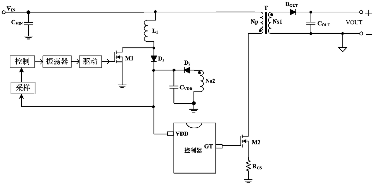
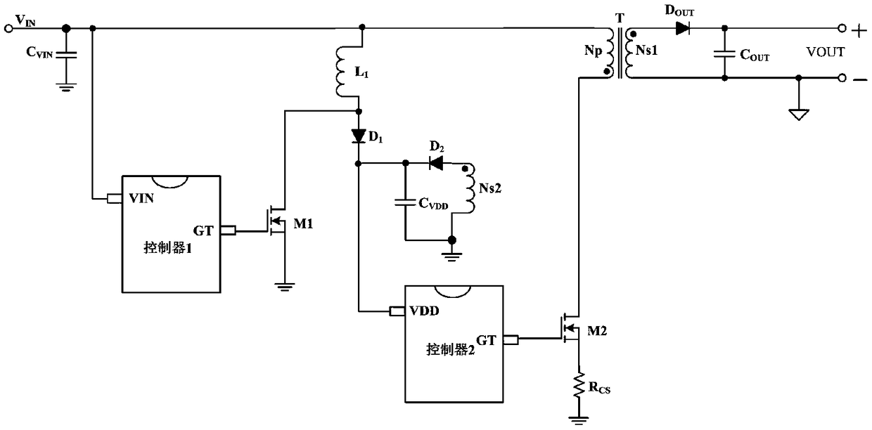
[0058] Figure 4 This is a simplified circuit diagram of the present invention in the application scenario of the optocoupler feedback flyback power supply, and the secondary side optocoupler, TL431 and loop compensation parts are omitted. The controller IC described in the present invention is a circuit in the controller 10, and other circuits in the controller 10 have nothing to do with the present invention, and will not be described here. Figure 4 The main power topology is known technology, including the input voltage V IN , output voltage V OUT , capacitor C VIN , C VDD and C OUT , controller 10, main power transformer, auxiliary winding Ns2, main power tube M1, diode D 1 , D 2 and D OUT , inductance L 1 and sampling resistor R CS and other components. The GT pin is the drive output of the controller 10, which is used to control the turn-on and turn-off of the power tube M1; the VDD pin is the power input pin of the controller 10, which is used for the power s...
Embodiment 2
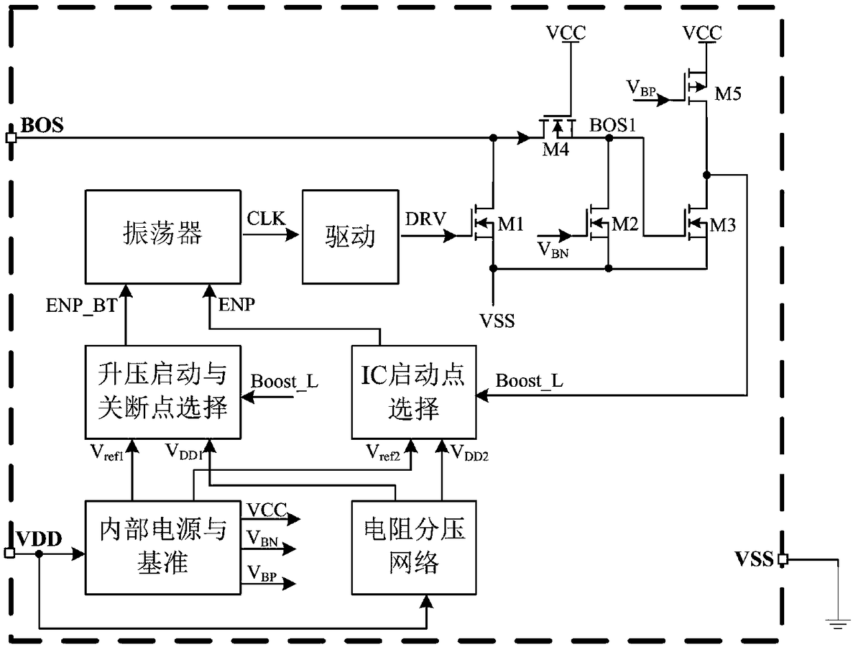
[0081] like Image 6 As shown, compared with the first embodiment, the difference is that the BOS end of the controller is externally connected to the ground, and the boost function is not implemented.
[0082] The basic working principle of this embodiment:
[0083] like Image 6 As shown, the BOS port of the controller is at the ground potential, so that the gate signal of the N-channel MOS transistor M3 is the ground potential, the MOS transistor M3 is not conducting, and its drain potential is pulled by the conduction of the P-channel MOS transistor M5 It becomes a high level, so that the output signal Boost_L is a high level, indicating that the boost function is invalid.
[0084] At this time, the Boost_L signal is input into the boost startup and shutdown point selection module, so that its output signal ENP_BT becomes low, and the enable is invalid; at the same time, the Boost_L signal is input into the IC startup point selection module, so that its output signal ENP...
PUM
 Abstract
Description
Claims
Application Information


