Narrow viewing angle display method
A display method and a narrow viewing angle technology, applied in the narrow viewing angle display field, can solve the problems of gray scale difference, gray scale inversion of anti-peep display, etc.
- Summary
- Abstract
- Description
- Claims
- Application Information
AI Technical Summary
Problems solved by technology
Method used
Image

Examples
no. 1 example
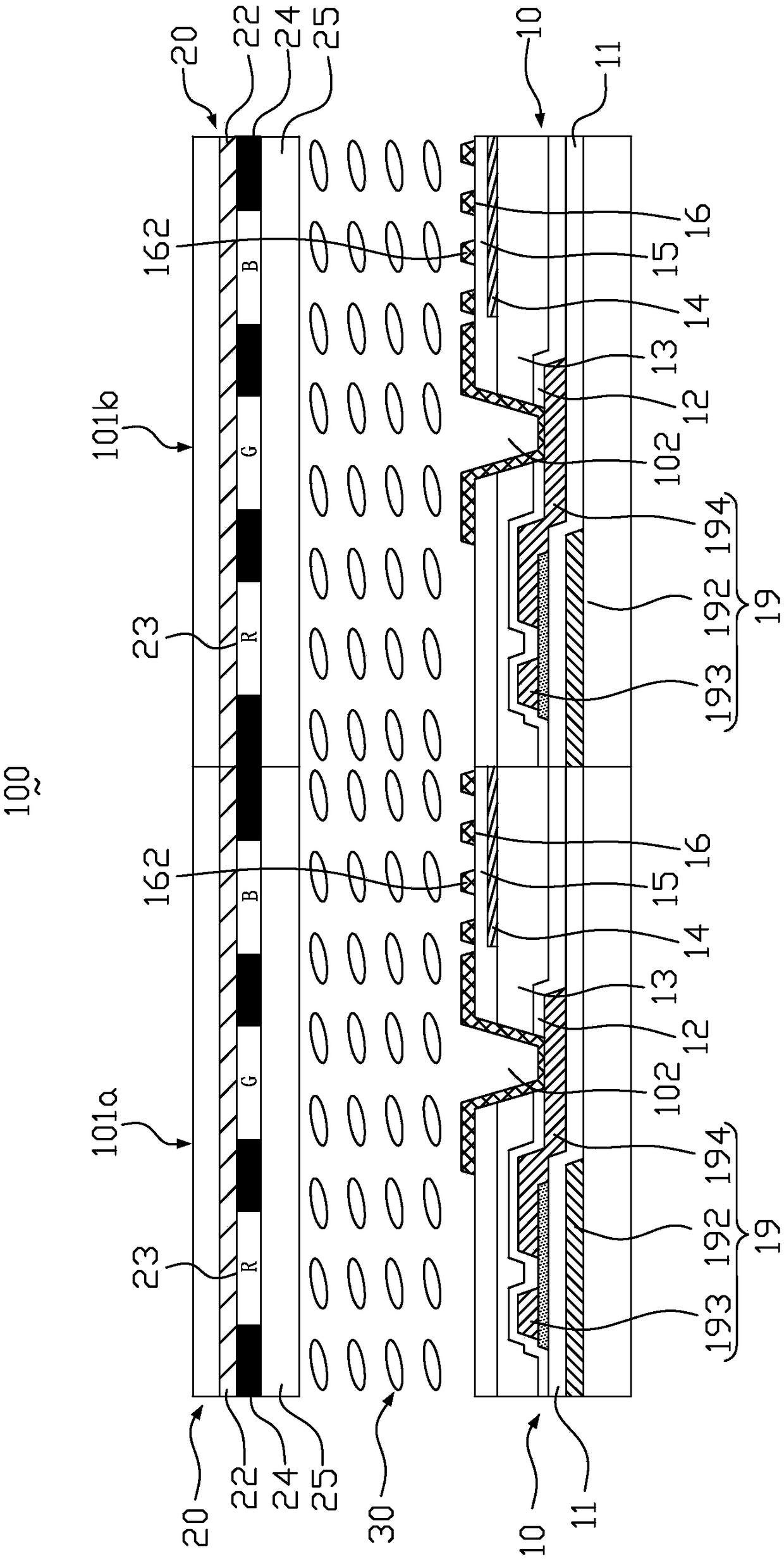
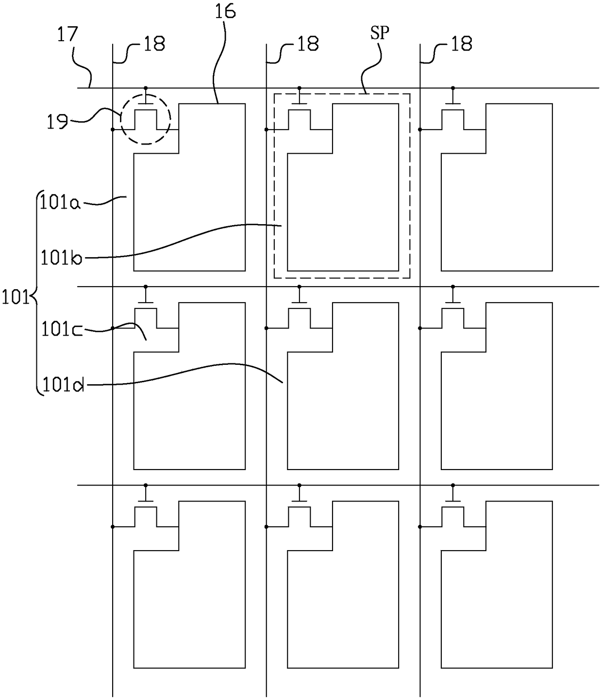
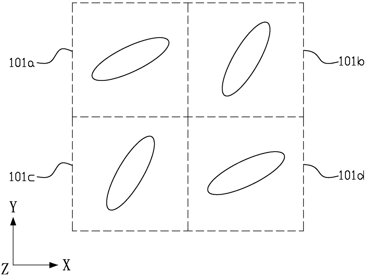
[0028] figure 1 is a schematic structural diagram of the display panel of the first embodiment of the present invention, figure 2 is a front view structural schematic diagram of the array substrate according to the first embodiment of the present invention. Such as figure 1 and figure 2 As shown, the display panel 100 of the present invention is an IPS or FFS liquid crystal display panel, that is, the common electrode 14 and the pixel electrode 16 are formed on the same substrate (ie, a thin film transistor array substrate). The IPS type display panel 100 will be described below. In this embodiment, the display panel 100 includes a plurality of pixels 101 arranged in a matrix, and each pixel 101 includes a first sub-pixel 101a, a second sub-pixel 101b, a third sub-pixel 101c, and a fourth sub-pixel 101d, and the first A sub-pixel 101a, a second sub-pixel 101b, a third sub-pixel 101c, and a fourth sub-pixel 101d are arranged in a matrix, wherein the first sub-pixel 101a i...
no. 2 example
[0037] Figure 4 is a schematic structural view of the color filter substrate according to the second embodiment of the present invention. Figure 5 is a front view structural diagram of the color filter substrate according to the second embodiment of the present invention. Such as Figure 4 and Figure 5 As shown, the structure of the display panel 100 of this embodiment is substantially the same as that of the display panel 100 of the first embodiment, except that the structure of the color filter substrate 20 is different.
[0038] Specifically, such as Figure 4 and Figure 5 As shown, the color filter substrate 20 is provided with a first anti-peeping electrode 22a, a second anti-peeping electrode 22b, a color resist layer 23, a black matrix 24 (BM), a flat layer 25 and an insulating layer 26 on the surface close to the liquid crystal layer 30 . The first anti-peeping electrode 22a is arranged on the color resist layer 23 and the black matrix 24; the insulating layer...
no. 3 example
[0045] Figure 9 is a schematic structural diagram of a display panel according to a third embodiment of the present invention. Such as Figure 9 As shown, the structure of the display panel 100 of this embodiment is substantially the same as that of the display panel 100 of the second embodiment, the difference lies in the partial structure of the color filter substrate 20 .
[0046] Specifically, the first privacy-preventing electrode 22a and the second privacy-preventing electrode 22b of the color filter substrate 20 are arranged on the color-resist layer 23 and the black matrix 24, that is, the first privacy-preventing electrode 22a and the second privacy-preventing electrode 22b are located The same layer of the substrate 20; the flat layer 25 covers the first peep prevention electrode 22a and the second peep prevention electrode 22b. Please refer to the second embodiment for the structures and functions of the first anti-peeping electrode 22a and the second anti-peepin...
PUM
 Abstract
Description
Claims
Application Information